Liquid crystal display panel and liquid crystal display device
A liquid crystal display panel, liquid crystal layer technology, applied in optics, instruments, nonlinear optics, etc., can solve problems such as incomplete curing of sealant and liquid crystal pollution
- Summary
- Abstract
- Description
- Claims
- Application Information
AI Technical Summary
Problems solved by technology
Method used
Image

Examples
no. 1 example
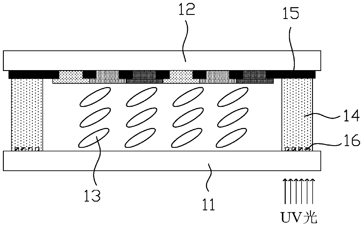
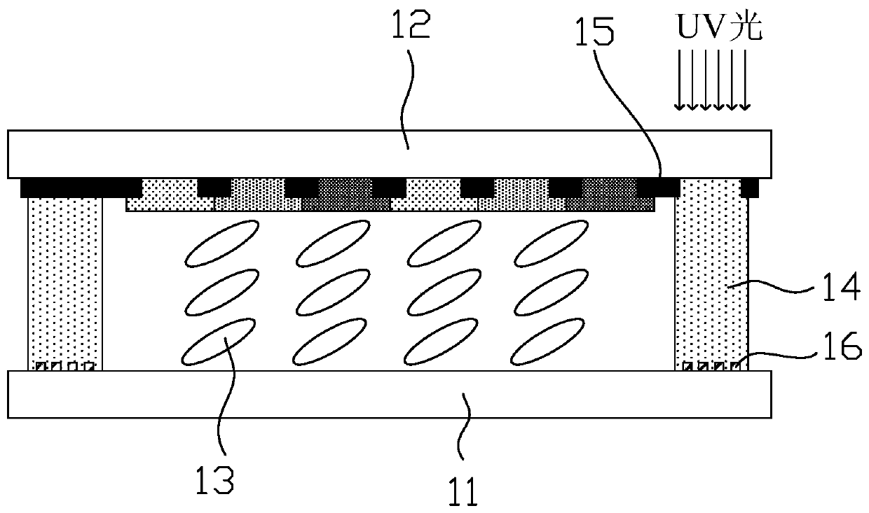
[0032] Please refer to image 3 , the first embodiment of the present invention provides a liquid crystal display panel, the liquid crystal display panel includes a first substrate 20 and a second substrate 30 oppositely arranged, a liquid crystal layer 40 located between the first substrate 20 and the second substrate 30 and a frame Glue 41. The liquid crystal display panel is provided with an effective display area (AA area) and a non-effective display area located on the periphery of the effective display area. During the manufacturing process of the liquid crystal display panel, the sealant 41 is coated on the first substrate 20 or the second substrate 30 in a circular manner. , and located in the non-effective display area, liquid crystal is dripped in the range limited by the ring sealant 41, and then the first substrate 20 and the second substrate 30 are opposed to form a box, and the sealant 41 is cured, so that the liquid crystal layer 40 It is packaged in a closed s...
no. 2 example
[0045] Please refer to Figure 5 , shows a schematic structural diagram of a liquid crystal display panel according to a second embodiment of the present invention. The difference from the above-mentioned first embodiment is that the through holes 310 are arranged in multiple rows in any horizontal side or vertical side, and the multiple rows of through holes 310 have specific layout rules.
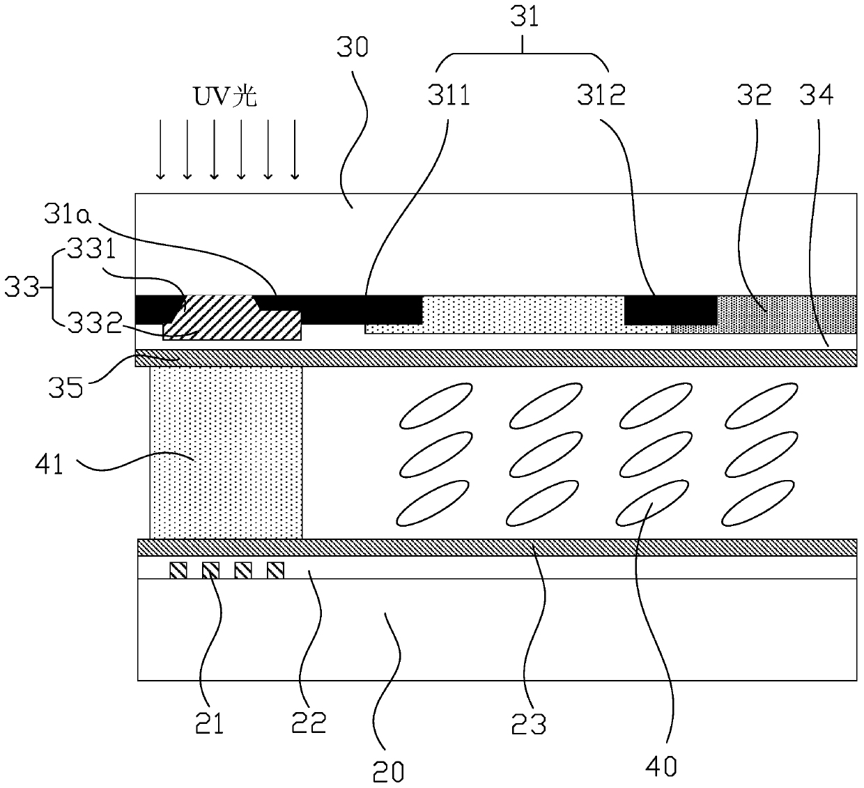
[0046] Specifically, see Image 6 , the black matrix 31 includes a first area A1, a second area A2 and a third area A3, the second area A2 is set on the side of the first area A1 close to the effective display area, and the third area A3 is set on the side of the first area A1 away from the effective display area. One side of the display area, that is, the edge portion 311 of the black matrix 31 includes a ring-shaped second area A2 , a first area A1 and a third area A3 from inside to outside.
[0047] The thickness of the black matrix 31 in the third area A3 is greater than the thickne...
no. 3 example
[0052] Please refer to Figure 9 , shows a schematic structural diagram of a liquid crystal display panel according to a third embodiment of the present invention. The difference from the above-mentioned first embodiment is that the liquid crystal display panel further includes an absorbing layer 36 located between the light diffusing layer 33 and the sealant 41, and the absorbing layer 36 includes dichroic dyes and liquid crystal molecules arranged in parallel to the axial direction. . Further, the first transparent insulating layer 22 is interposed between the absorption layer 36 and the metal circuit 21 , and the first alignment layer 23 covers the absorption layer 36 . Preferably, the width of the overlapping portion of the absorbing layer 36 and the sealant 41 is 0.5-0.95 times the width of the sealant 41 , and the width of the absorbing layer 36 is greater than or equal to the width of the sealant 41 .
[0053] When the liquid crystal display panel is produced and disp...
PUM
| Property | Measurement | Unit |
|---|---|---|
| thickness | aaaaa | aaaaa |
| thickness | aaaaa | aaaaa |
Abstract
Description
Claims
Application Information
 - R&D
- Intellectual Property
- Life Sciences
- Materials
- Tech Scout
- Unparalleled Data Quality
- Higher Quality Content
- 60% Fewer Hallucinations
Browse by: Latest US Patents, China's latest patents, Technical Efficacy Thesaurus, Application Domain, Technology Topic, Popular Technical Reports.
© 2025 PatSnap. All rights reserved.Legal|Privacy policy|Modern Slavery Act Transparency Statement|Sitemap|About US| Contact US: help@patsnap.com