Multilayer circuit board structure

A multi-layer circuit board and circuit board technology, which is applied in the structural connection of printed circuits, printed circuits, circuit heating devices, etc., can solve the problems of long working hours, complicated manufacturing processes, and many parts, and achieve the goal of reducing process steps and working hours Effect

Active Publication Date: 2020-04-17
CHICONY ELECTRONICS
View PDF15 Cites 0 Cited by
  • Summary
  • Abstract
  • Description
  • Claims
  • Application Information

AI Technical Summary

Problems solved by technology

It can be seen that in the past, the stacking structure of multi-layer circuit boards required many parts to be assembled, that is, multiple screw fixing bases were required to be screwed one by one to lock the two circuit boards and the heat sink was assembled between the two circuit boards. and other steps, resulting in complex manufacturing process and long working hours

Method used


Image

  • Multilayer circuit board structure
  • Multilayer circuit board structure
  • Multilayer circuit board structure

Examples


Embodiment Construction

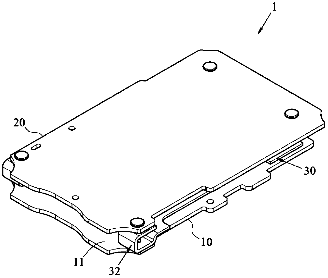
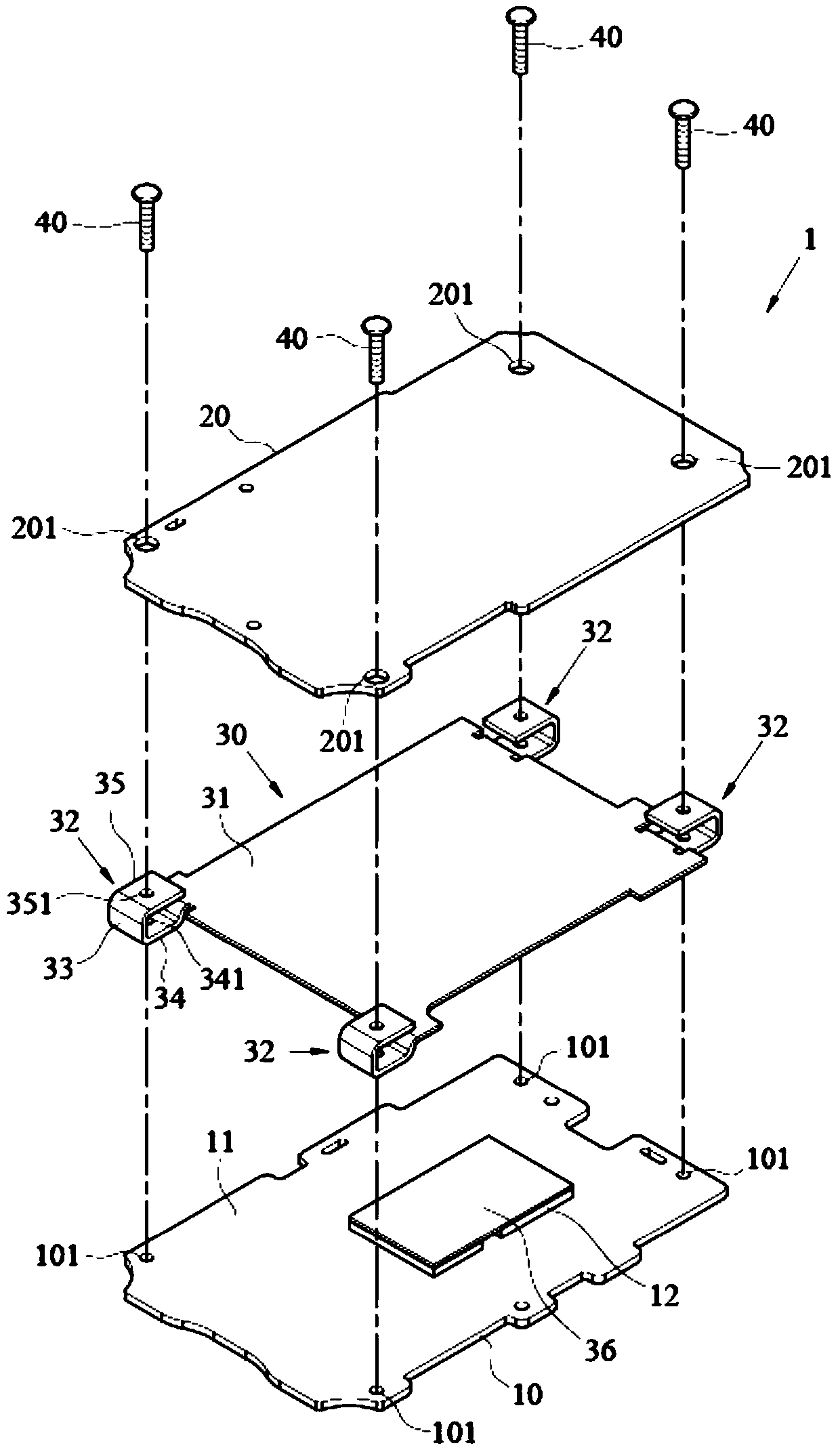
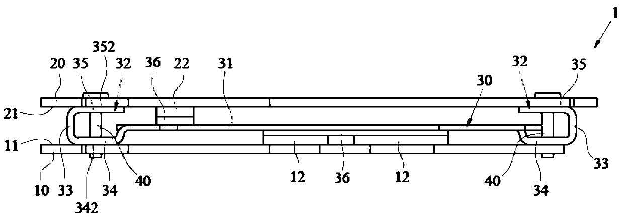
[0013] figure 1 It is a perspective view of the first embodiment of the multilayer circuit board structure of the present invention, figure 2 It is an exploded perspective view of the first embodiment of the multilayer circuit board structure of the present invention, image 3 It is a side view of the first embodiment of the multilayer circuit board structure of the present invention. Such as Figure 1 to Figure 3 As shown, the multilayer circuit board structure 1 can be a circuit board structure with more than two layers. For example, in this embodiment, the multilayer circuit board structure 1 is a double layer circuit board structure and includes a first circuit board 10, a second circuit board 20 and cooling plate 30. In some embodiments, the multilayer circuit board structure 1 can be applied to various electronic products, such as smart phones, tablet computers, notebook computers, video cameras or digital cameras, and the like.

[0014] Such as Figure 1 to Figure...


PUM


Abstract

The invention discloses a multilayer circuit board structure. The multilayer circuit board structure comprises a first circuit board, a second circuit board and a heat dissipation plate, wherein the first circuit board includes a first surface; the second circuit board includes a second surface facing the first surface; the heat dissipation plate is located between the first circuit board and thesecond circuit board; the heat dissipation plate comprises a substrate and a fixing base; the fixing base is formed by integrally bending and extending the substrate; the fixing base comprises a connecting plate, a first plate and a second plate, a distance is kept between the first plate and the second plate, and the connecting plate is connected between the first plate and the second plate; thefirst surface of the first circuit board is combined with the surface of the first board; the second surface of the second circuit board is combined with the surface of the second board; and the substrate is not contacted with the first surface and the second surface.

Description

technical field [0001] The present invention relates to a circuit board structure, in particular to a multilayer circuit board structure. Background technique [0002] With the advancement of technology, the functions of electronic products are becoming more and more diversified. However, due to the current trend of thinning and thinning electronic products, in order to configure more electronic components in a limited space, some electronic products will Adapted by stacking multi-layer circuit boards. [0003] The stacked structure of multi-layer circuit boards currently on the market is mainly arranged between two circuit boards through a plurality of screw fixing seats, and the screws pass through the two circuit boards and are screwed to the screw fixing seats respectively, so that the two circuit boards The boards can be stacked and fixed on the opposite two sides of the plurality of screw fixing bases to keep the distance. In addition, a cooling device is assembled b...

Claims


Application Information

Patent Timeline
Patent Type & Authority Applications(China)
IPC IPC(8): H05K1/02H05K1/14
CPCH05K1/0209H05K1/144
Inventor 陈威铮张津恺
Owner CHICONY ELECTRONICS
Why Eureka
Try Eureka