

Preparation method of OLED light-emitting substrate and OLED light-emitting device
A substrate and film layer technology, which is applied in the manufacture of semiconductor devices, electrical solid devices, semiconductor/solid devices, etc., can solve the problems of uneven interface morphology, insufficient compactness, and uneven film formation of the ink layer Smooth appearance, improve compactness and uniformity, and improve film formation
- Summary
- Abstract
- Description
- Claims
- Application Information
AI Technical Summary
Problems solved by technology
Method used
Image

Examples
Embodiment Construction
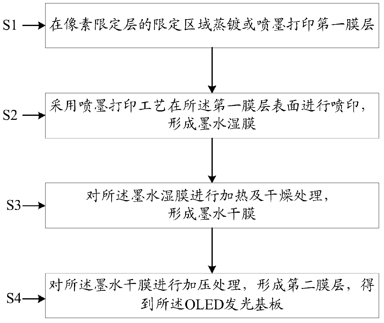
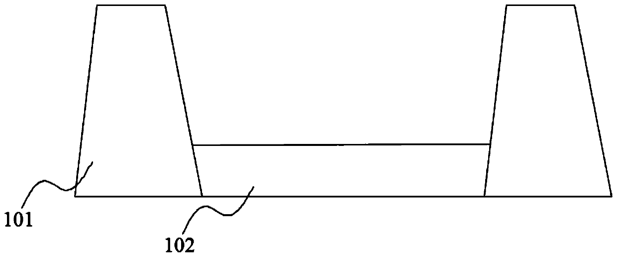
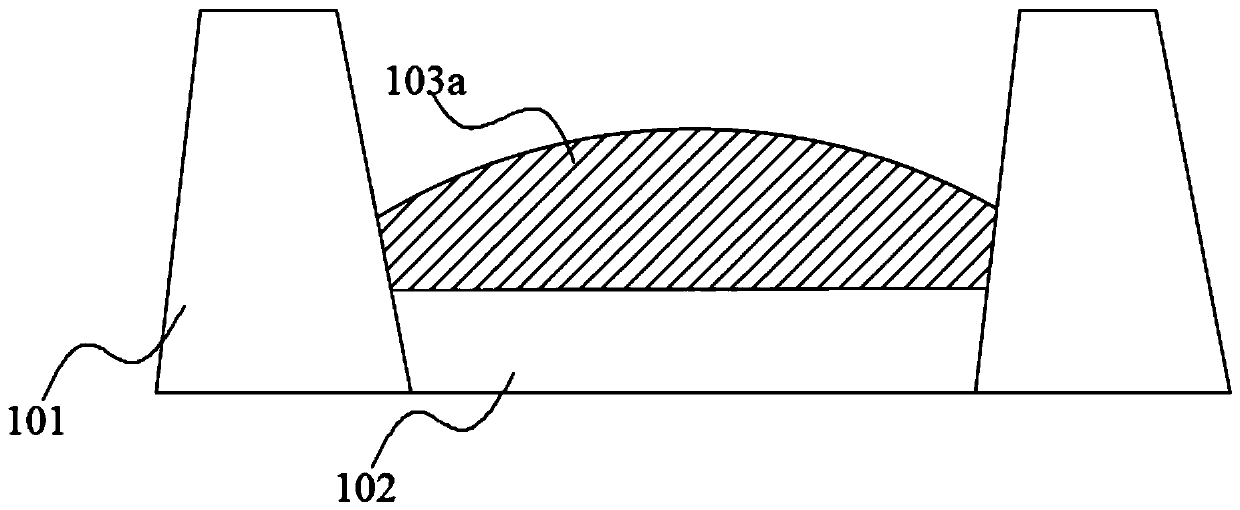
[0027] The following will clearly and completely describe the technical solutions in the embodiments of the present invention with reference to the drawings in the embodiments of the present invention. Apparently, the described embodiments are only some of the embodiments of the present invention, but not all of them. Based on the embodiments of the present invention, all other embodiments obtained by those skilled in the art without creative efforts fall within the protection scope of the present invention.
[0028] In describing the present invention, it should be understood that the terms "center", "longitudinal", "transverse", "length", "width", "thickness", "upper", "lower", "front", " Orientation indicated by rear, left, right, vertical, horizontal, top, bottom, inside, outside, clockwise, counterclockwise, etc. The positional relationship is based on the orientation or positional relationship shown in the drawings, which is only for the convenience of describing the pr...
PUM
 Abstract
Description
Claims
Application Information