A small-volume three-dimensional antifuse FPGA online debugging and verification method
A verification method and anti-fuse technology, applied in the direction of instruments, measuring devices, measuring electronics, etc., can solve problems such as hardware design incompatibility, and achieve the effects of proving reliability, reducing space, and reducing volume
- Summary
- Abstract
- Description
- Claims
- Application Information
AI Technical Summary
Problems solved by technology
Method used
Image
Examples
Embodiment
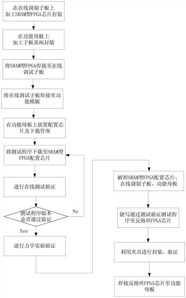
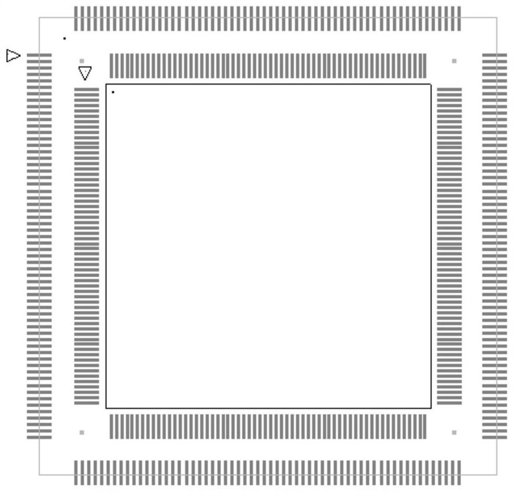
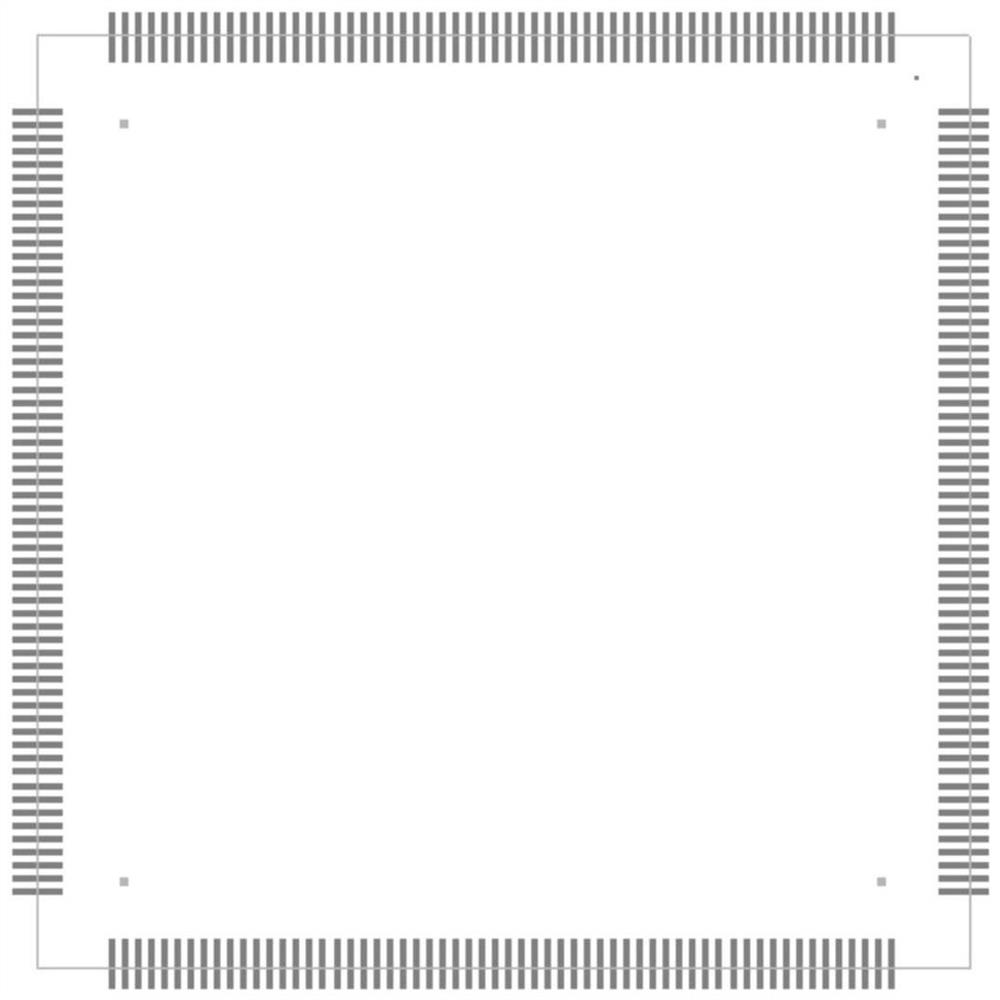
[0061] The surface-mount pads associated with the chip are designed on the front side of the online debugging sub-board, and the size and spacing of the surface-mount pads on the back side of the square board are in one-to-one correspondence with the front pads. The size of the pads is SMD90REC14, and the pad spacing is 24mil. A 6mil via hole is drilled on the group pad to realize the connection of the front and back pads. The model of the SRAM FPGA chip is EPF10K70RI240, and the model of the antifuse FPGA chip is A54SX72A-1CQ208B. The SRAM type FPGA configuration chip model is EPC2. The online verification method is compatible with domestic devices of the same type.
[0062] In the same way, the verification method of CGA packaging is an example: the model of the FLASH FPGA chip is A3PE3000, and the model of the antifuse FPGA chip is AX2000. The online verification method is compatible with domestic devices of the same type.
PUM
 Abstract
Description
Claims
Application Information


