a photodetector

A photodetector and spectroscopic technology, applied in the field of photodetectors, can solve the problems of obvious saturable absorption effect, low responsivity, and incompatibility with silicon technology.

Active Publication Date: 2021-07-06
WUHAN OPTICAL VALLEY INFORMATION OPTOELECTRONICS INNOVATION CENT CO LTD
View PDF5 Cites 0 Cited by
  • Summary
  • Abstract
  • Description
  • Claims
  • Application Information

AI Technical Summary

Problems solved by technology

However, the energy band structure of crystalline silicon materials determines that its detection efficiency in the optical communication band is very low. Although III-V semiconductor materials are more suitable for photodetectors, III-V semiconductor materials are not compatible with silicon technology and cannot be used with silicon Carry out effective monolithic integration; Considering the compatibility of germanium material and CMOS process, the technology of using germanium material as light absorbing layer material to form germanium silicon photodetector has been proposed in this field
However, the current silicon germanium photodetectors have the disadvantages of obvious saturated absorption effect and low responsivity, so further improvement is needed

Method used


Image

  • a photodetector
  • a photodetector
  • a photodetector

Examples


Embodiment Construction

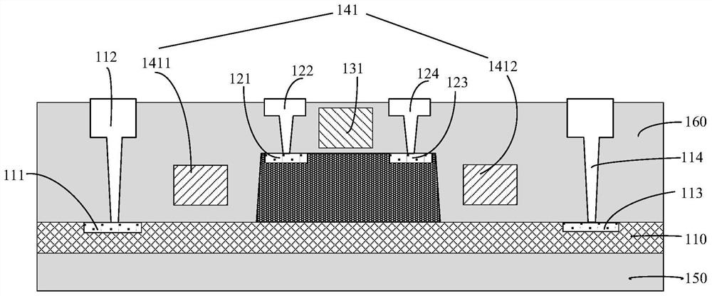
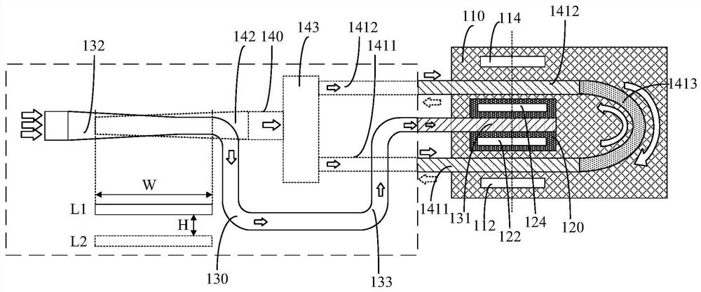
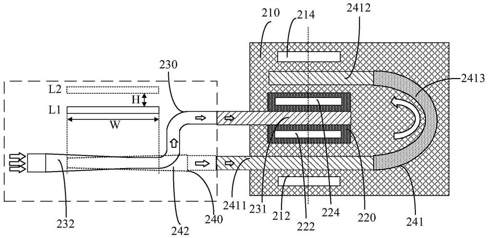
[0028] Exemplary embodiments disclosed in the present application will be described in more detail below with reference to the accompanying drawings. Although exemplary embodiments of the present application are shown in the drawings, it should be understood that the present application may be embodied in various forms and should not be limited to the specific embodiments set forth herein. Rather, these embodiments are provided for a more thorough understanding of the present application and for fully conveying the scope disclosed in the present application to those skilled in the art.

[0029] In the following description, numerous specific details are given in order to provide a more thorough understanding of the present application. It will be apparent, however, to one skilled in the art that the present application may be practiced without one or more of these details. In other examples, in order to avoid confusion with the present application, some technical features kno...


PUM

PropertyMeasurementUnit
lengthaaaaaaaaaa
lengthaaaaaaaaaa
widthaaaaaaaaaa

Abstract

In order to solve the problem that the existing photodetector has obvious saturated absorption effect and low responsivity, an embodiment of the present application provides a photodetector, which relates to the technical field of photodetectors. The photodetector includes: a silicon layer, the The silicon layer includes a doped region of the first doping type; a germanium layer in contact with the silicon layer, the germanium layer includes a doped region of the second doping type; a first layer waveguide, the first layer waveguide includes A first detection coupling region disposed above the germanium layer; a second layer waveguide, the second layer waveguide including a second detection coupling region disposed on the side of the germanium layer; wherein, the first layer waveguide and the second layer waveguide The second-layer waveguide is used to transmit optical signals, and the first-layer waveguide and the second-layer waveguide respectively couple the optical signal to the a germanium layer; the germanium layer is used to detect the optical signal and convert the optical signal into an electrical signal.

Description

technical field [0001] The embodiments of the present application relate to the technical field of photodetectors, and in particular to a photodetector. Background technique [0002] Silicon photonics technology is a new generation of optical device development and integration based on silicon and silicon-based substrate materials (such as SiGe / Si, silicon-on-insulator, etc.) using existing complementary metal oxide semiconductor (Complementary Metal Oxide Semiconductor, CMOS) technology technology. Silicon photonics technology combines the characteristics of ultra-large-scale and ultra-high-precision manufacturing of integrated circuit technology with the advantages of ultra-high speed and ultra-low power consumption of photonic technology. It is a disruptive technology to cope with the failure of Moore's Law. This combination benefits from the scalability of semiconductor wafer fabrication, thereby reducing costs. As one of the core devices of silicon photonics architect...

Claims


Application Information

Patent Timeline
Patent Type & Authority Patents(China)
IPC IPC(8): H01L31/109H01L31/0232
CPCH01L31/0232H01L31/109
Inventor 胡晓肖希王磊陈代高张宇光李淼峰
Owner WUHAN OPTICAL VALLEY INFORMATION OPTOELECTRONICS INNOVATION CENT CO LTD
Why Eureka
Try Eureka