Bulk acoustic wave resonator having void layer on electrode, method of manufacturing same, filter, and electronic apparatus

A technology of bulk acoustic wave resonators and resonators, applied in the direction of electrical components, impedance networks, etc., can solve problems such as reduction, Q value reduction of resonators, and deterioration of bulk acoustic wave filter performance of bulk acoustic wave resonators, etc.

Pending Publication Date: 2020-05-08
ROFS MICROSYST TIANJIN CO LTD
View PDF0 Cites 8 Cited by
  • Summary
  • Abstract
  • Description
  • Claims
  • Application Information

AI Technical Summary

Problems solved by technology

For bulk acoustic wave resonators and filters, high operating frequency means that the film thickness, especially that of the electrode, needs to be further reduced; however, the main negative effect brought about by the reduction of the electrode film thickness is the resonator Q due to the increase in electrical loss. value decreases, especially the Q value at the series resonance point and its frequency vicinity; correspondingly, the performance of high operating frequency bulk acoustic wave filter is also greatly deteriorated with the decrease of the Q value of the bulk acoustic wave resonator

Method used


Image

  • Bulk acoustic wave resonator having void layer on electrode, method of manufacturing same, filter, and electronic apparatus
  • Bulk acoustic wave resonator having void layer on electrode, method of manufacturing same, filter, and electronic apparatus
  • Bulk acoustic wave resonator having void layer on electrode, method of manufacturing same, filter, and electronic apparatus

Examples


Embodiment Construction

[0040] The technical solutions of the present invention will be further described in detail below through embodiments and in conjunction with the accompanying drawings. In the specification, the same or similar reference numerals refer to the same or similar parts. The following description of the embodiments of the present invention with reference to the accompanying drawings is intended to explain the general inventive concept of the present invention, and should not be construed as a limitation of the present invention.

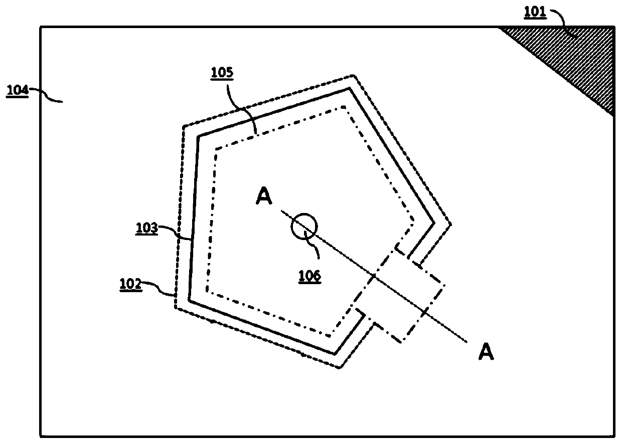
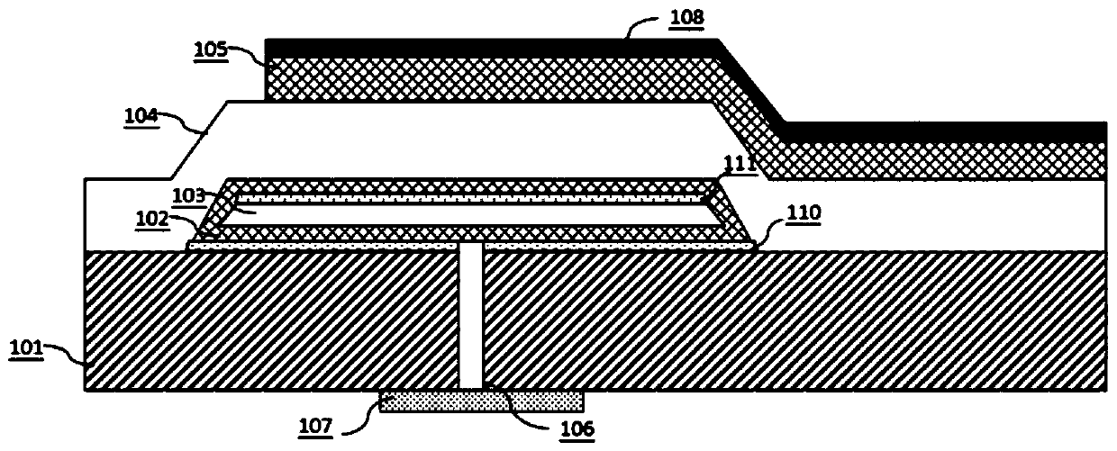
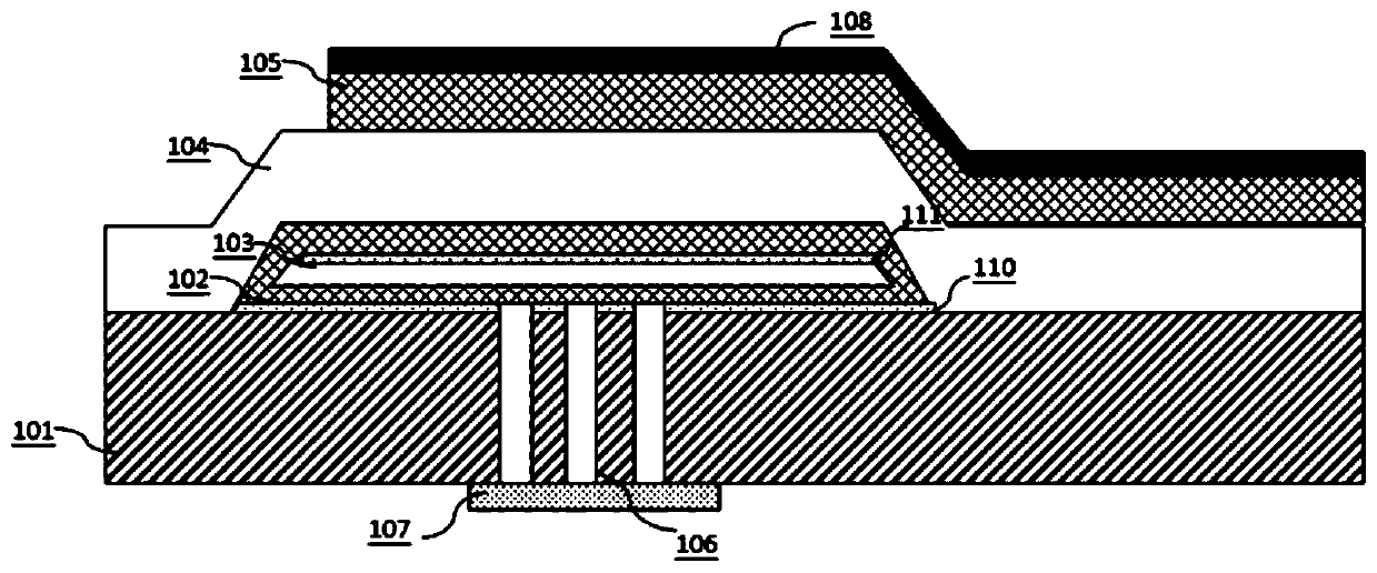
[0041] figure 1 is a schematic top view of a bulk acoustic wave resonator according to an exemplary embodiment of the present invention, Figure 1A for the edge according to an exemplary embodiment of the present invention figure 1 A schematic cross-sectional view taken along the A-A direction. exist figure 1 and Figure 1A , the reference numerals are as follows:

[0042] 101: Substrate, optional materials are single crystal silicon, gallium arsenid...


PUM


Abstract

The invention relates to a bulk acoustic wave resonator and a manufacturing method thereof. The resonator includes: a substrate; a bottom electrode; a top electrode; and a piezoelectric layer, the electrode is arranged between the bottom electrode and the top electrode; wherein the bottom electrode is a gap electrode, the gap electrode is provided with a gap layer, distances exist between the gaplayer and the top surface and the bottom surface of the gap electrode in the thickness direction of the gap electrode, the gap layer forms an acoustic mirror cavity of the resonator, or an acoustic mirror structure is arranged in the gap layer; the substrate is provided with at least one electric connection through hole, one end of the through hole is connected to the bottom electrode, and the other end of the through hole is suitable for being connected to a bonding pad located on the lower side of the substrate. The invention further relates to a filter with the resonator and electronic apparatus with the filter or the resonator.

Description

technical field [0001] Embodiments of the present invention relate to the field of semiconductors, and in particular, to a bulk acoustic wave resonator and a method for manufacturing the same, a filter having the resonator, and an electronic device having the resonator or the filter. Background technique [0002] As the basic elements of electronic equipment, electronic devices have been widely used, and their applications include mobile phones, automobiles, home appliances and so on. In addition, technologies such as artificial intelligence, the Internet of Things, and 5G communications that will change the world in the future still need to rely on electronic devices as their foundation. [0003] Electronic devices can play different characteristics and advantages according to different working principles. Among all electronic devices, devices that use the piezoelectric effect (or inverse piezoelectric effect) are one of the most important categories. Piezoelectric devices ...

Claims


Application Information

Patent Timeline
Patent Type & Authority Applications(China)
IPC IPC(8): H03H9/02H03H9/17H03H3/02
CPCH03H9/02H03H9/17H03H3/02H03H9/173H03H9/131H03H2003/021
Inventor 徐洋庞慰班圣光孔庆路
Owner ROFS MICROSYST TIANJIN CO LTD
Why Eureka
Try Eureka