Chip structure and manufacturing method thereof

A chip structure, n-type technology, applied in semiconductor devices, electrical components, circuits, etc., can solve the problems of low compound efficiency of ultraviolet LEDs, large electron leakage of ultraviolet LEDs, etc., to improve quantum efficiency and light extraction efficiency. The effect of large numbers, increasing the probability of radiative recombination

Active Publication Date: 2021-09-24
GUANGDONG INST OF SEMICON IND TECH
View PDF9 Cites 0 Cited by
  • Summary
  • Abstract
  • Description
  • Claims
  • Application Information

AI Technical Summary

Problems solved by technology

[0005] The purpose of this application is to provide a chip structure and its manufacturing method to solve the problem of relatively large electron leakage in ultraviolet LEDs in the prior art, resulting in low recombination efficiency of ultraviolet LEDs

Method used


Image

  • Chip structure and manufacturing method thereof
  • Chip structure and manufacturing method thereof
  • Chip structure and manufacturing method thereof

Examples


no. 1 example

[0049] As mentioned in the background art, compared with more mature blue LEDs, ultraviolet LEDs still exhibit lower radiation recombination efficiency and light extraction efficiency. Limiting the output of higher quantum efficiency of ultraviolet optoelectronic devices is mainly due to the lower hole injection efficiency and greater electron leakage in the active region, which is more obvious in deep ultraviolet light-emitting devices with shorter wavelengths, which in turn leads to higher Lower carrier concentration and lower radiative recombination efficiency in the low quantum well. Hole injection is more difficult, the mass of holes is relatively large, and the migration speed in the active region is relatively slow, while the leakage of electrons reduces the recombination efficiency of electrons and holes.

[0050] In view of this, the present application provides a chip structure. By adding an n-type electron storage layer in the chip structure, it is possible to provi...

no. 2 example

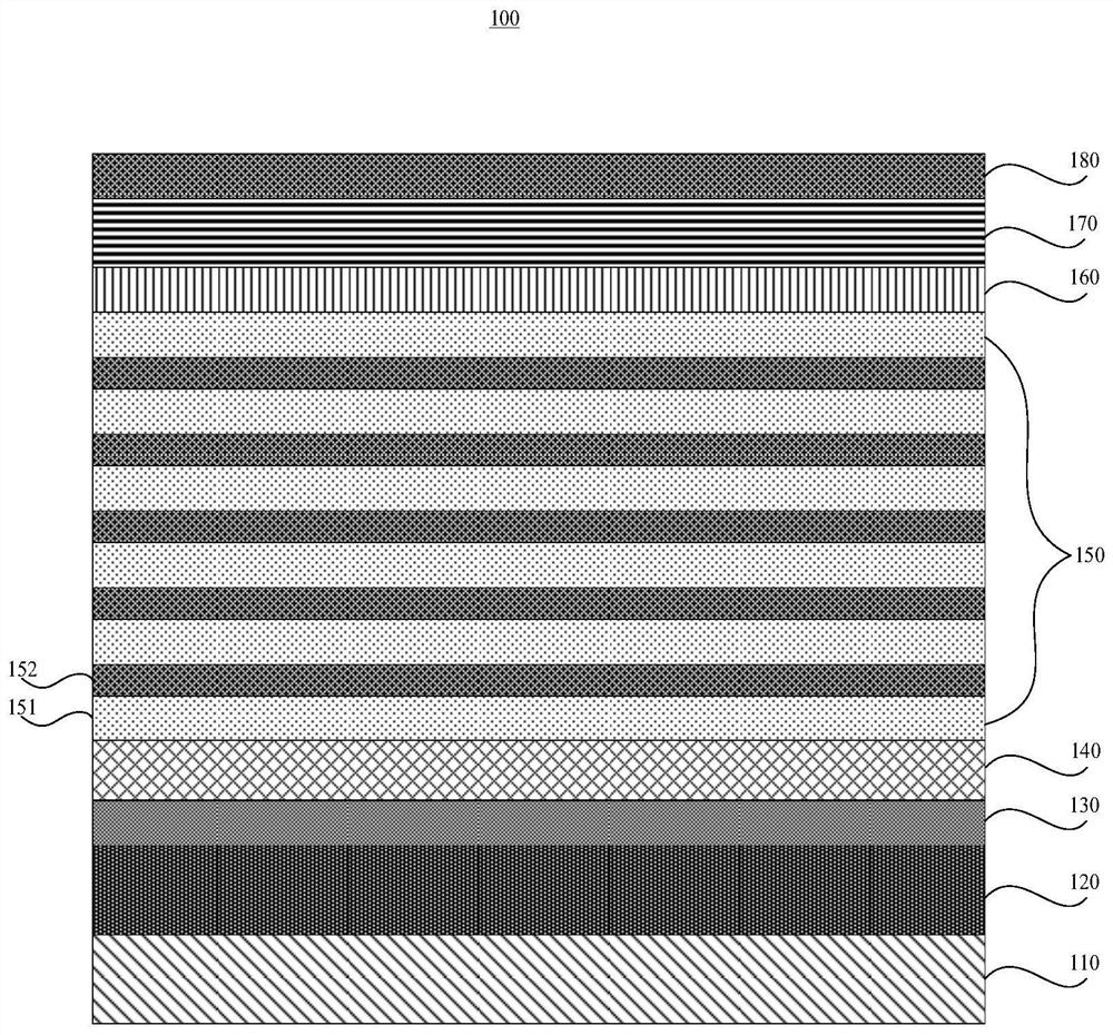
[0070] The embodiment of the present application also provides a chip structure manufacturing method, the method is used to manufacture the chip structure 100 described in the first embodiment, the method includes:

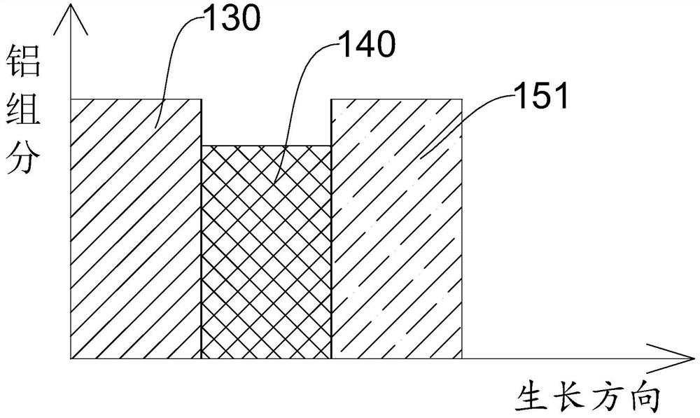
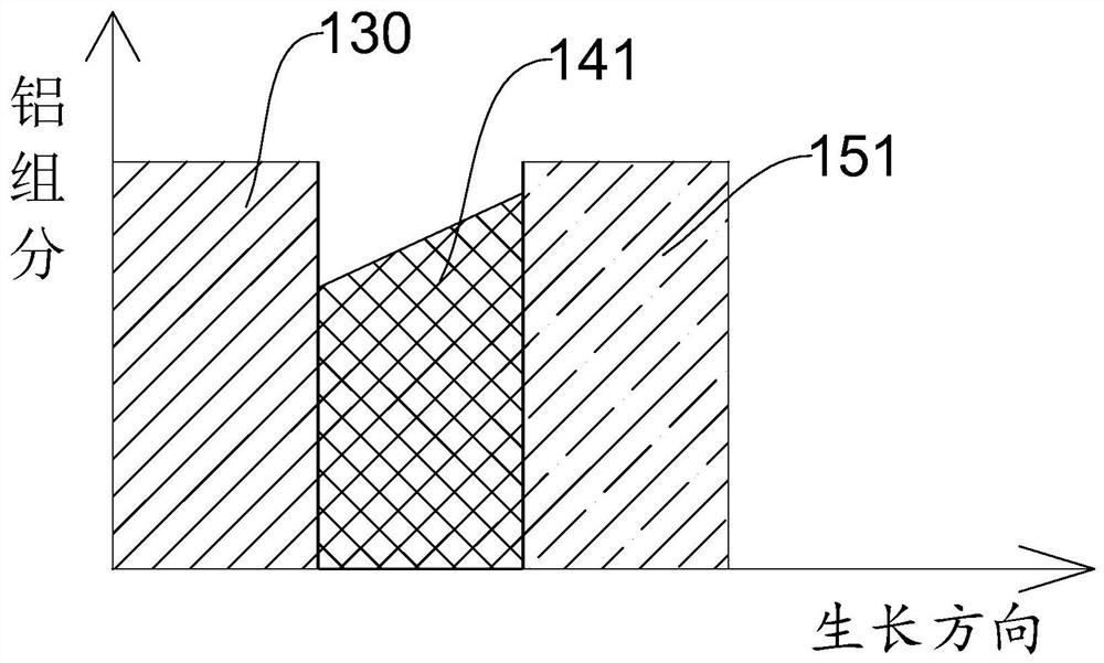
[0071] Growing buffer layer 120, n-type semiconductor layer 130, n-type electron storage layer 140 sequentially along the surface of a substrate 110, Al x Ga 1-x N / Al y Ga 1-y N light-emitting active region, p-type electron blocking layer, p-type semiconductor layer 170 and contact layer 180, and 0.01≤x

[0072] Wherein, the step of growing the n-type electron storage layer 140 includes:

[0073] In the reaction chamber, adjust the temperature to the target temperature, and adjust the flow rate of the Al source and the Ga source to gradually change with the growth time, so as to grow the n-type electron storage layer 140 with a gradually changing aluminum composition;

[0074] Or adjust the flows of the Al source and the Ga source to be constant with the ...


PUM


Abstract

The application provides a chip structure and a manufacturing method thereof, which relate to the field of semiconductors. The chip structure includes a substrate, a buffer layer, an n-type semiconductor layer, an n-type electron storage layer, and an Al x Ga 1‑x N / Al y Ga 1‑y N light-emitting active region, p-type electron blocking layer, p-type semiconductor layer and contact layer, and 0.01≤x

Description

technical field [0001] The present application relates to the field of semiconductors, in particular, to a chip structure and a manufacturing method thereof. Background technique [0002] In recent years, AlGaN-based ultraviolet LED (Light Emitting Diode, light-emitting diode) has the advantages of environmental protection, mercury-free, sterilization, high modulation frequency, etc. The field has important commercial application value. [0003] However, compared with more mature blue LEDs, UV LEDs still show lower radiation recombination efficiency and light extraction efficiency. Limiting the output of higher quantum efficiency of ultraviolet optoelectronic devices is mainly due to the lower hole injection efficiency and greater electron leakage in the active region, which is more obvious in deep ultraviolet light-emitting devices with shorter wavelengths, which in turn leads to higher Lower carrier concentration and lower radiative recombination efficiency in the low qu...

Claims


Application Information

Patent Timeline
Patent Type & Authority Patents(China)
IPC IPC(8): H01L33/20H01L33/32H01L33/14H01L33/00
CPCH01L33/0075H01L33/14H01L33/145H01L33/20H01L33/325
Inventor 王巧刘宁炀卢汉伦梁锡辉王君君
Owner GUANGDONG INST OF SEMICON IND TECH
Why Eureka
Try Eureka