Array substrate, preparation method thereof and display device
A technology for array substrates and display areas, which is applied in semiconductor/solid-state device manufacturing, instruments, semiconductor devices, etc., and can solve problems such as misoperation and easy conduction of electrostatic discharge units
- Summary
- Abstract
- Description
- Claims
- Application Information
AI Technical Summary
Problems solved by technology
Method used
Image

Examples
no. 1 example
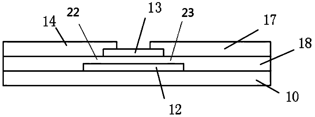
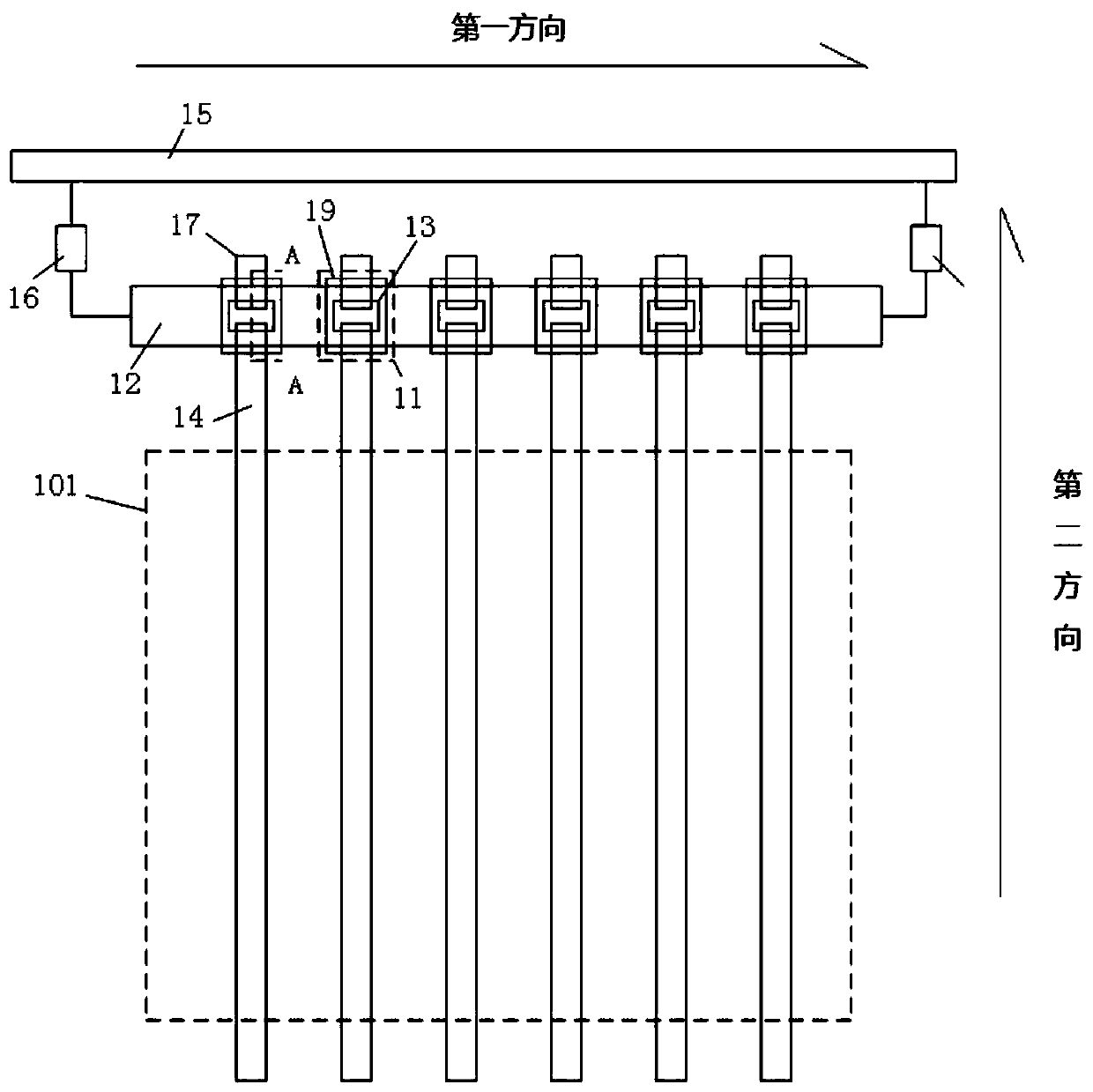
[0038] figure 1 is a schematic structural diagram of the first embodiment of the array substrate of the present invention; figure 2 for figure 1 Sectional view at A-A in the middle. Such as figure 1 and figure 2 As shown, the array substrate provided in this embodiment is an array substrate. The array substrate includes a substrate 10 and a first electrostatic discharge unit 11 disposed on the substrate 10. The first electrostatic discharge unit 11 includes a substrate formed on the substrate 10. The electrostatic discharge line 12 , the active layer 13 disposed on the electrostatic discharge line 12 and the data line 14 disposed on the active layer 13 , the data line 14 is connected to the active layer 13 . The data line 14 at least partially overlaps and is spaced apart from the ESD line 12 to form a first capacitor 22 . Wherein, the substrate 10 is a glass substrate, and the electrostatic discharge line 12 is a gate metal layer.
[0039] In the embodiment, the elect...
no. 2 example
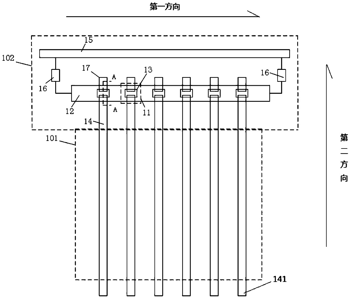
[0049] image 3 is a schematic structural diagram of the second embodiment of the array substrate of the present invention; Figure 4 for image 3 Sectional view at A-A in the middle. Such as image 3 and Figure 4 As shown, this embodiment is an extension of the aforementioned first embodiment, and the main structure of the array substrate of this embodiment is basically the same as that of the aforementioned first embodiment, the difference is that the electrostatic discharge line 12 extends along the first direction A plurality of active layers 13 are arranged at intervals on the electrostatic discharge line 12, and the active layers 13 are arranged at intervals along the first direction. A plurality of data lines 14 are arranged at intervals along the first direction on the substrate 10 , and the data lines 14 correspond to the active layers 13 one by one. The data lines 14 extend along the second direction, and each data line 14 extends above the active layer 13 . E...
no. 3 example
[0055] Figure 5 is a schematic structural diagram of the third embodiment of the array substrate of the present invention; Figure 6 for Figure 5 Sectional view at B-B in middle. Such as Figure 5 and Figure 6 As shown, this embodiment is an extension of the aforementioned second embodiment, and the main structure of the array substrate of this embodiment is basically the same as that of the aforementioned second embodiment, the difference is that the electrostatic discharge line 12 extends along the first direction A plurality of active layers 13 are arranged at intervals on the electrostatic discharge line 12, and the active layers 13 are arranged at intervals along the first direction. A plurality of data lines 14 are arranged at intervals along the first direction on the substrate 10 , and the data lines 14 correspond to the active layers 13 one by one. The data lines 14 extend along the second direction, and each data line 14 extends above the active layer 13 . E...
PUM
 Abstract
Description
Claims
Application Information