Printed circuit board processing method and printed circuit board
A technology of printed circuit boards and processing methods, which is applied in the direction of printed circuit, printed circuit, printed circuit manufacturing, etc., can solve the problems of large demand, high production cost, and many process procedures, so as to improve productivity, reduce production cost, reduce The effect of the process
- Summary
- Abstract
- Description
- Claims
- Application Information
AI Technical Summary
Problems solved by technology
Method used
Image

Examples
Embodiment Construction
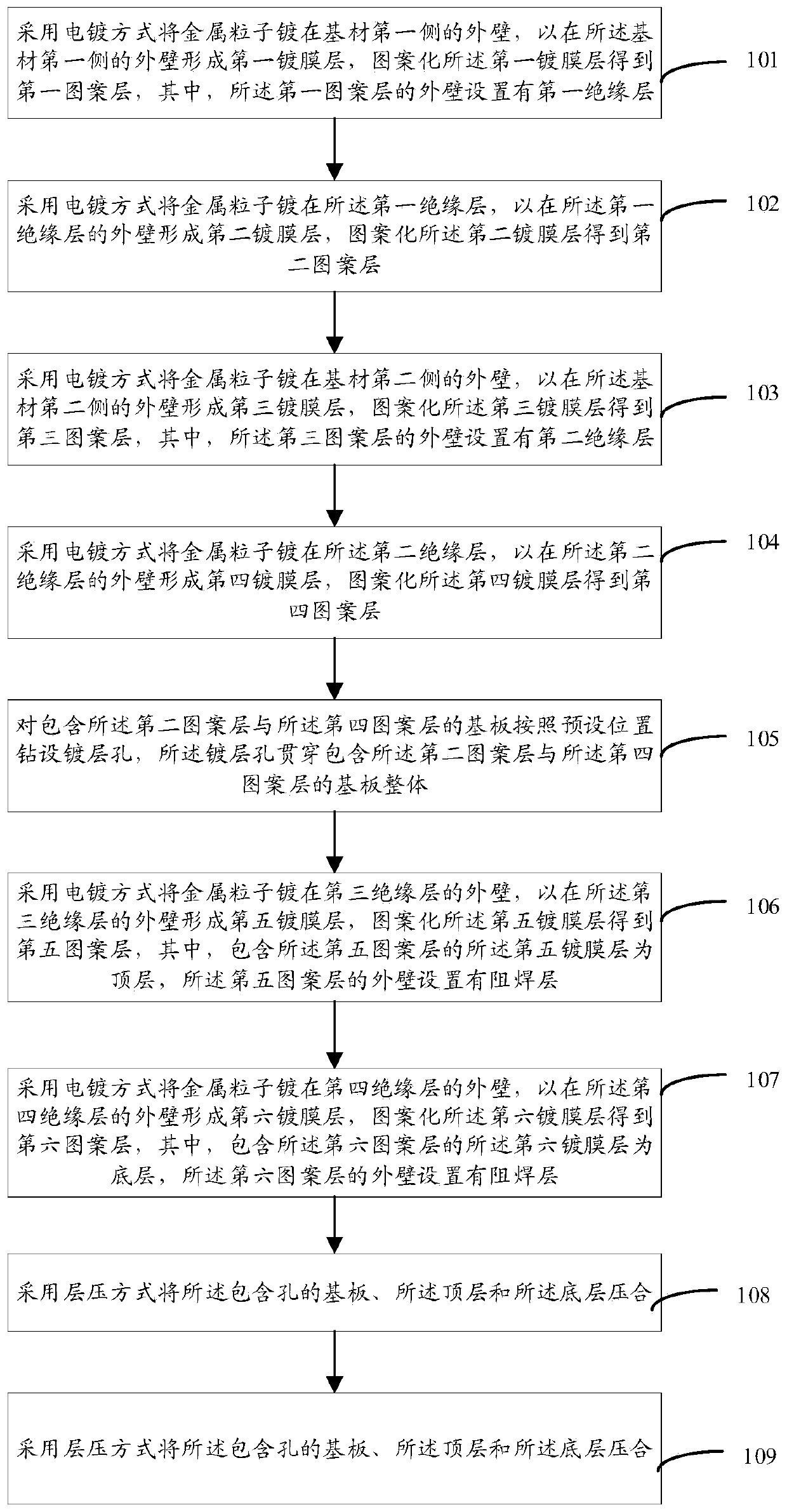
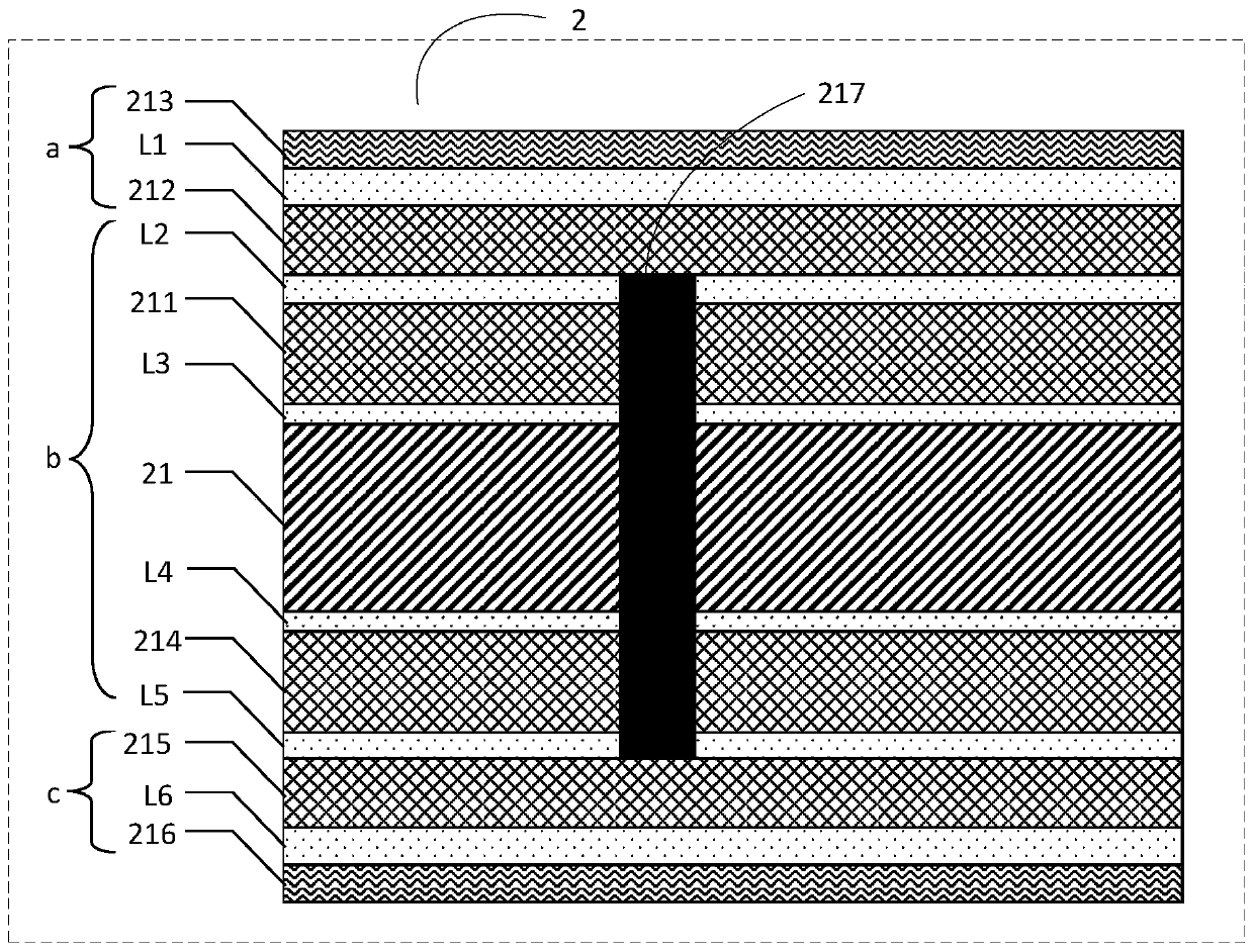
[0032] The terms "first" and "second" in the description and claims of the embodiments of the present application and the above drawings are used to distinguish similar objects, but not necessarily used to describe a specific sequence or sequence. It is to be understood that the terms so used are interchangeable under appropriate circumstances such that the embodiments described herein are capable of practice in sequences other than those illustrated or described herein. The following will clearly and completely describe the technical solutions in the embodiments of the application with reference to the drawings in the embodiments of the application. Apparently, the described embodiments are only some of the embodiments of the application, not all of them. Based on the embodiments in this application, all other embodiments obtained by those skilled in the art without making creative efforts belong to the scope of protection of this application.
[0033] The technical solutions...
PUM
| Property | Measurement | Unit |
|---|---|---|
| Thickness | aaaaa | aaaaa |
| Thickness | aaaaa | aaaaa |
| Thickness | aaaaa | aaaaa |
Abstract
Description
Claims
Application Information
PatSnap Eureka turns technology decisions into work you can execute. Powered by our Innovation Knowledge Graph, it runs expert workflows across engineering, life sciences, materials and intellectual property. Get your review-ready output in minutes.


