Supercharge Your Innovation With Domain-Expert AI Agents!

Processing method of a laminate

A processing method and a laminated body technology, applied in metal processing equipment, manufacturing tools, electrical solid devices, etc., can solve problems such as quality reduction, image sensor chip defects, etc.

Active Publication Date: 2020-05-26
DISCO CORP
View PDF9 Cites 0 Cited by
  • Summary
  • Abstract
  • Description
  • Claims
  • Application Information

AI Technical Summary

Problems solved by technology

[0007] When the laminated body is divided by the technology described in the above-mentioned Patent Document 1, there is a problem that defects are generated on the outer periphery of the image sensor chip on the wafer side, resulting in a decrease in quality. When the laminate is divided, there is a problem that dust falls from the modified layer of the wafer constituting the laminate and adheres to the image sensor chip, resulting in a decrease in quality.

Method used


Image

  • Processing method of a laminate
  • Processing method of a laminate
  • Processing method of a laminate

Examples


Embodiment Construction

[0023] Hereinafter, the processing method of the laminated body which concerns on embodiment of this invention is demonstrated in detail, referring drawings.

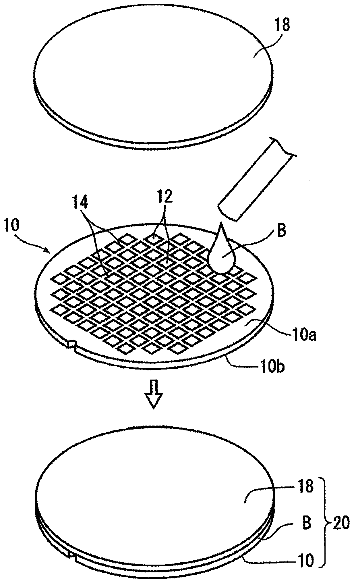
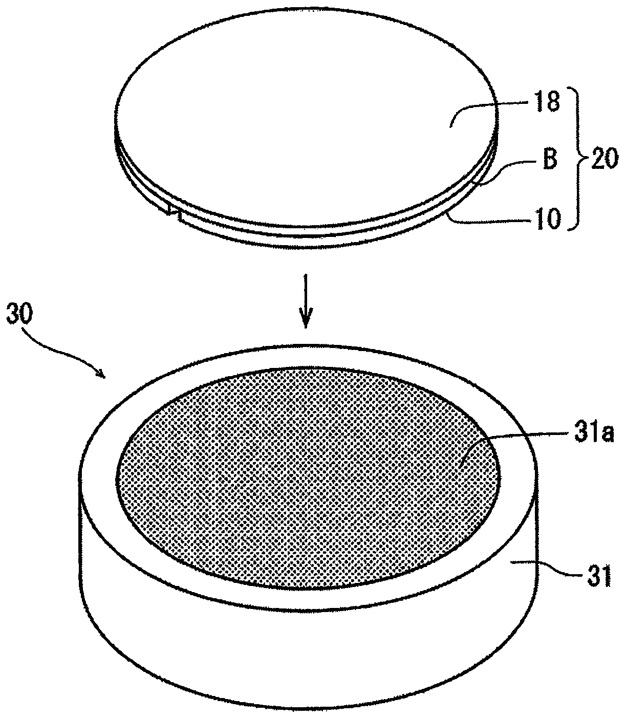
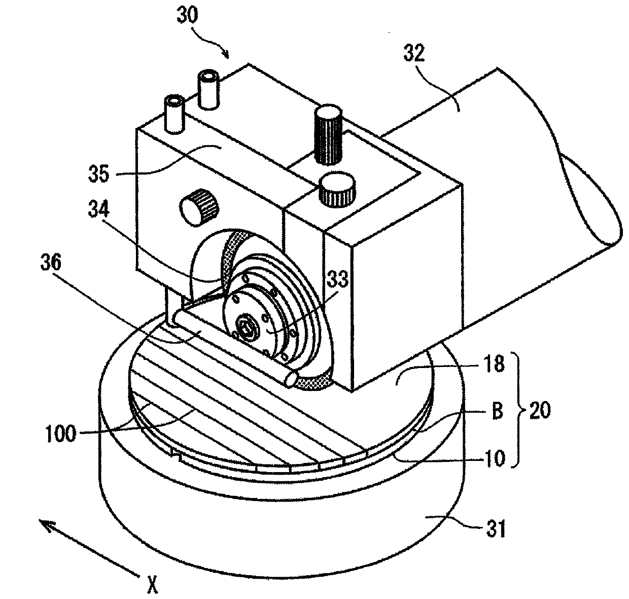
[0024] Such as figure 1 As shown, first, for example, a wafer 10 made of silicon (Si) and a transparent glass substrate 18 are prepared. The wafer 10 is divided by a plurality of intersecting dividing lines 14 and a plurality of image sensors (CMOS) 12 are formed on the front surface 10a. . Once the wafer 10 and the glass substrate 18 are prepared, a transparent adhesive (resin bond) B is dropped on the front surface 10 a of the wafer 10 to bond the glass substrate 18 . In this way, the wafer 10 and the glass substrate 18 are integrated through the adhesive layer B composed of the above-mentioned adhesive B to form a laminated body 20 (refer to figure 1 lower part of ).

[0025] (cutting groove forming process)

[0026] Once the laminated body 20 is formed as described above, the cutting groove forming step is perfo...


PUM

PropertyMeasurementUnit
frequencyaaaaaaaaaa

Abstract

A laminate processing method includes a modified layer removing step of positioning a cutting blade to the region of the wafer corresponding to each of the division lines and cutting while supplying cutting water into which a water-soluble resin is mixed from the wafer side of the laminate, thereby removing the modified layer formed inside the wafer, a dividing step of, after the modified layer removing step is carried out, expanding the expandable tape, and dividing the laminate into individual image sensor chips, and a cleaning step of supplying cleaning water from the back surface of the wafer with a state in which the expandable tape is expanded being maintained, thereby cleaning the laminate.

Description

technical field [0001] The present invention relates to a method of processing a laminated body, which divides the laminated body in which a glass substrate is arranged on the front surface of a wafer via a transparent adhesive layer into individual image sensor chips. Background technique [0002] Divided by a plurality of intersecting dividing lines and formed with a plurality of image sensors such as CMOS and CCD on the upper surface of a semiconductor substrate such as silicon, the wafer is passed through a dicing device with a cutting tool in a rotatable manner, or with a laser light condensing device. A laser processing device for a concentrator that performs processing on a workpiece is divided into individual image sensor chips, and the divided image sensor chips are used in digital cameras, mobile phones, microscopes, and the like. [0003] Since the imaging function of the image sensor is reduced due to dust, scratches, etc., a transparent body such as glass is arr...

Claims


Application Information

Patent Timeline
Patent Type & Authority Applications(China)
IPC IPC(8): H01L21/78H01L27/146B23K26/53
CPCH01L27/14687H01L27/14698H01L21/78B23K26/53B23K2103/56H01L21/6838H01L21/67092H01L21/67132H01L21/67115H01L21/6836H01L2221/68327H01L2221/6834H01L21/6835H01L2221/68336H01L21/3043H01L27/14683H01L21/76H01L21/02052H01L21/67028H01L2221/6839
Inventor 中村胜
Owner DISCO CORP
Features
  • R&D
  • Intellectual Property
  • Life Sciences
  • Materials
  • Tech Scout
  • Unparalleled Data Quality
  • Higher Quality Content
  • 60% Fewer Hallucinations
Learn More