TVS device with low trigger voltage and manufacturing method of TVS device

A device manufacturing method and low trigger voltage technology, which are applied in the direction of electric solid devices, electrical components, semiconductor devices, etc., can solve the problems of high turn-on voltage, burnout and failure of the subsequent circuit chips, and inability to protect the subsequent circuit chips. Capacitance, effect of small turn-on voltage

Pending Publication Date: 2020-06-02
SHANGHAI CHANGYUAN WAYON MICROELECTRONICS
View PDF0 Cites 0 Cited by
  • Summary
  • Abstract
  • Description
  • Claims
  • Application Information

AI Technical Summary

Problems solved by technology

[0004] TVS devices with ordinary SCR structure are limited by the traditional structure and process, and the turn-on voltage is often high
Although the TVS can turn on and protect the subsequent circuit when encountering a high voltage pulse, when encountering a voltage pulse that is lower than the TVS turn-on voltage and higher than the withstand voltage of the subsequent circuit chip, the TVS device cannot be turned on due to failure. Protect the back-stage circuit chip, and eventually cause the back-stage circuit chip to burn out and fail

Method used


Image

  • TVS device with low trigger voltage and manufacturing method of TVS device
  • TVS device with low trigger voltage and manufacturing method of TVS device
  • TVS device with low trigger voltage and manufacturing method of TVS device

Examples


Embodiment Construction

[0047] The technical solutions in the embodiments of the present invention will be clearly and completely described below in conjunction with the accompanying drawings in the embodiments of the present invention. Apparently, the described embodiments are only some of the embodiments of the present invention, not all of them. Based on the embodiments of the present invention, all other embodiments obtained by persons of ordinary skill in the art without making creative efforts all belong to the protection scope of the present invention.

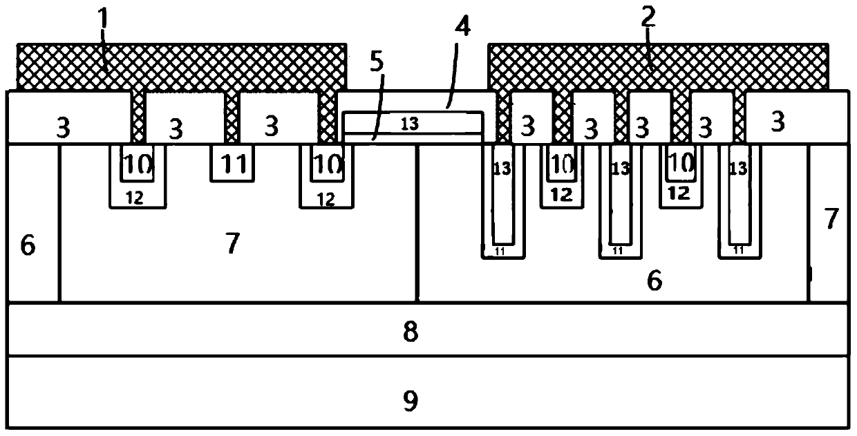
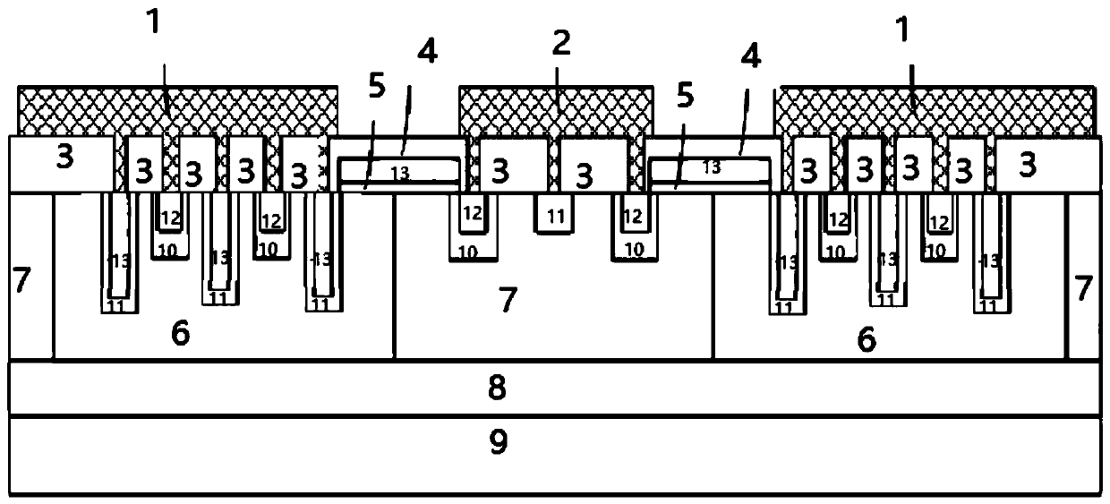
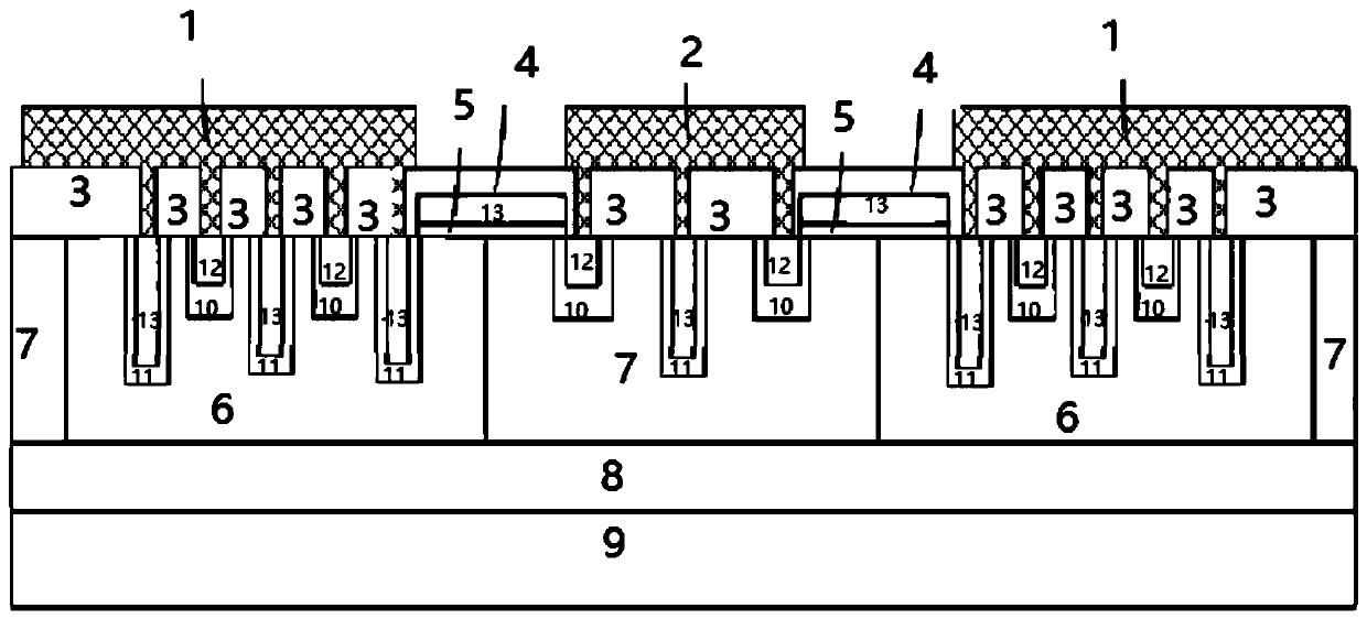
[0048] Such as Figure 1-14 As shown, the present invention provides a TVS with a low trigger voltage and a method of manufacturing the same.

[0049] Please refer to Figure 4 , the structure of a TVS device in the embodiment of the present invention has a layer of N-type buried layer 8 on the P-type substrate layer, a P-type epitaxial layer is grown on the N-type buried layer 8, and several layers are arranged above the P-type epitaxial lay...


PUM

PropertyMeasurementUnit
electrical resistivityaaaaaaaaaa
thicknessaaaaaaaaaa
electrical resistivityaaaaaaaaaa

Abstract

The invention provides a TVS device with low trigger voltage and a manufacturing method of the TVS device. An N-type buried layer is arranged on a P-type substrate layer; a P-type epitaxial layer grows on the N-type buried layer; a plurality of N well regions and P well regions are arranged above the P-type epitaxial layer; a plurality of deep grooves are formed in the surfaces of the N well region and the P well region; a plurality of N+ regions and P+ regions are respectively formed in the deep grooves; N+ polycrystalline silicon is deposited in at least one N+ region; a PLD region is formedin at least one P+ region; an oxide layer is arranged above the N well region and the P well region; first N+ polycrystalline silicon is arranged on the outer surface of the oxide layer; a first dielectric layer is arranged on the outer surface of the N+ polycrystalline silicon; and a plurality of second dielectric layers are deposited on the P-type epitaxial layer, contact holes are formed in the dielectric layers, and at least one cathode and at least one anode are respectively deposited on the contact holes. According to the invention, the trigger voltage of the device can be reduced, andthe characteristic of extremely low on-resistance of the device is kept.

Description

technical field [0001] The invention belongs to the technical field of semiconductor protection devices, in particular to a TVS device with low trigger voltage and a manufacturing method thereof. Background technique [0002] Transient Voltage Suppressors (TVS for short) is a commonly used protection device, which has extremely fast response speed and considerable surge discharge capability. When it is subjected to a momentary high-energy surge or electrostatic shock, TVS can change the impedance value between the two ends from high impedance to low impedance at a very high speed, so as to discharge a momentary large current, and at the same time reduce the voltage across the two ends. It is clamped at a small value to protect the downstream circuit chip from the impact of transient high-voltage surge pulses, so TVS is an essential protection device. [0003] Usually, devices such as diodes, triodes, GGNMOS (gate-grounded NMOS), and SCR are used as protection units of TVS d...

Claims


Application Information

Patent Timeline
Patent Type & Authority Applications(China)
IPC IPC(8): H01L29/06H01L27/02
CPCH01L27/0262H01L29/0615H01L29/0688
Inventor 蒋骞苑苏海伟赵德益李洪赵志方吕海凤张啸王允张彩霞
Owner SHANGHAI CHANGYUAN WAYON MICROELECTRONICS
Why Eureka
Try Eureka