LED epitaxial growth method for reducing dislocation density of quantum well

A technology of epitaxial growth and quantum well, which is applied in the direction of electrical components, circuits, semiconductor devices, etc., can solve the problems of quantum well dislocation defects, low luminous efficiency, and high leakage of LED devices, so as to reduce the growth rate of GaN and improve the crystal quality , The effect of improving luminous efficiency

Inactive Publication Date: 2020-06-02
XIANGNENG HUALEI OPTOELECTRONICS
View PDF3 Cites 1 Cited by
  • Summary
  • Abstract
  • Description
  • Claims
  • Application Information

AI Technical Summary

Problems solved by technology

[0006] In view of this, the purpose of the present invention is to provide a LED epitaxial growth method that reduces the dislocation density of quantum wells, and solve

Method used


Image

  • LED epitaxial growth method for reducing dislocation density of quantum well
  • LED epitaxial growth method for reducing dislocation density of quantum well
  • LED epitaxial growth method for reducing dislocation density of quantum well

Examples


Example Embodiment

[0044] Example 1:

Example Embodiment

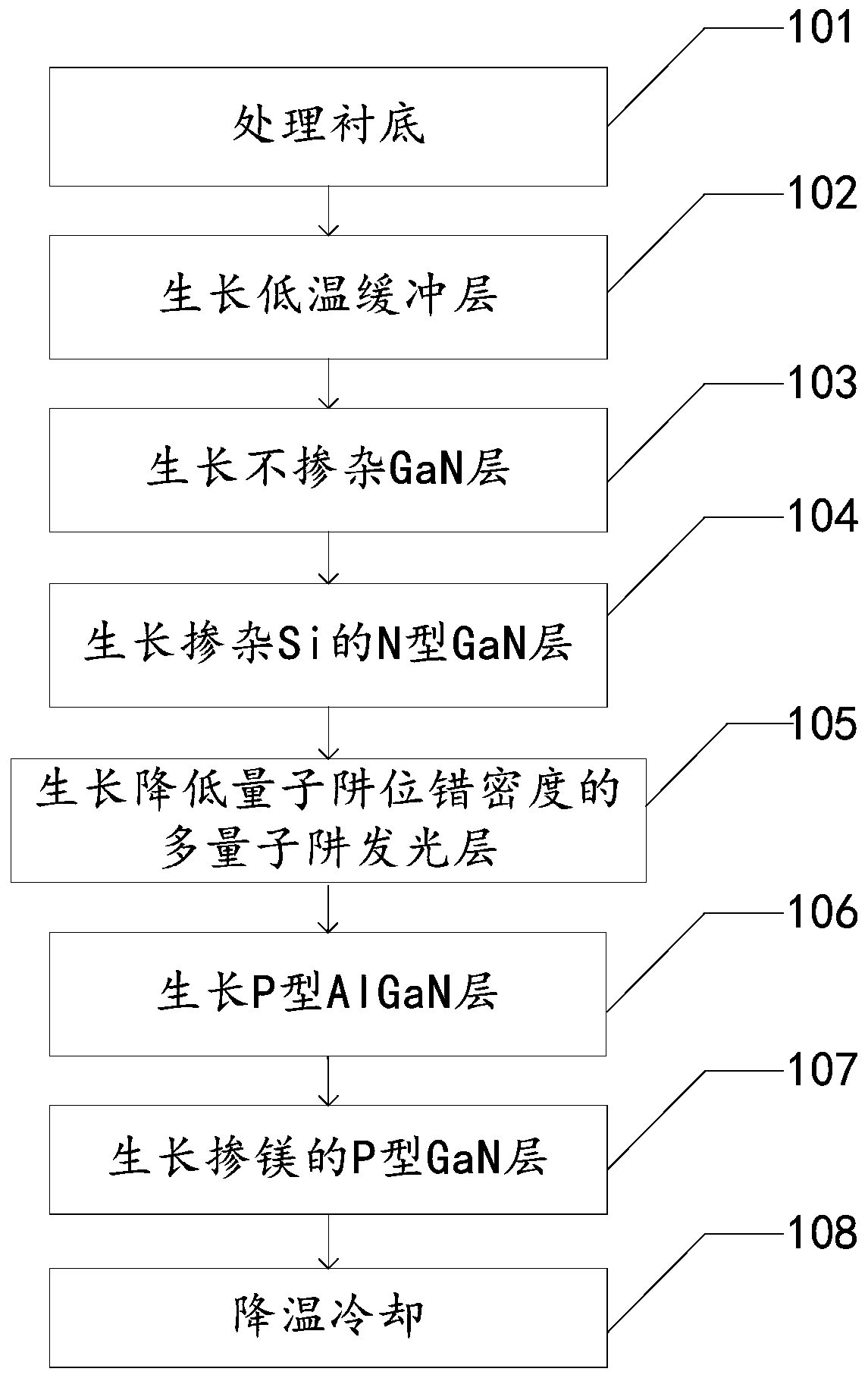
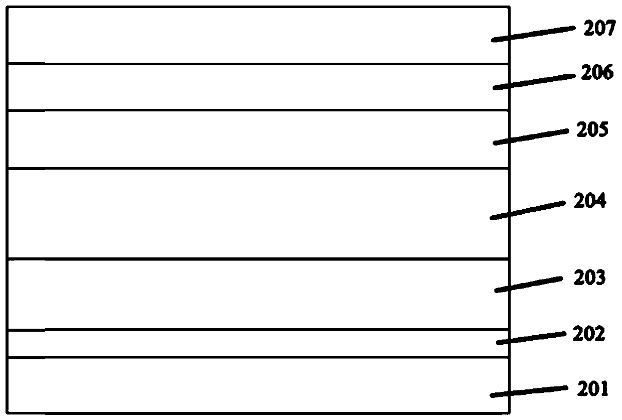
[0045] In this embodiment, MOCVD is used to grow high-brightness GaN-based LED epitaxial wafers, and high-purity H 2 Or high purity N 2 Or high purity H 2 And high purity N 2 Mixed gas as carrier gas, high purity NH 3 As the N source, trimethylgallium (TMGa) as the gallium source, trimethylindium (TMIn) as the indium source, silane (SiH 4 ) As the N-type dopant, trimethyl aluminum (TMAl) as the aluminum source, and magnesium cerene (CP 2 Mg) is used as the P-type dopant, the substrate is faceted sapphire, and the pressure of the reaction chamber is between 150 mbar and 600 mbar. See figure 1 Shown is a specific embodiment of the LED epitaxial growth method for reducing the dislocation density of quantum wells according to the application, and the method includes:

[0046] Step 101: processing the sapphire substrate, specifically, processing the sapphire substrate for 5-10 minutes under a hydrogen atmosphere at a temperature of 1000-1020°C and a pressure controlled at 100-150mbar.

...

Example Embodiment

[0058] Example 2:

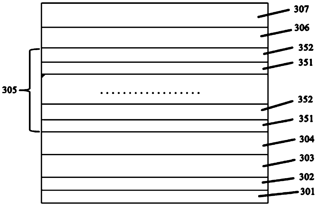
[0059] Such as Figure 4 As shown, the schematic flow chart of the LED epitaxial growth method for reducing the dislocation density of the quantum well in this embodiment, the method includes:

[0060] In step 401, the sapphire substrate is processed, specifically, the sapphire substrate is processed for 5-10 minutes in a hydrogen atmosphere at a temperature of 1000-1020°C and a pressure controlled at 100-150mbar.

[0061] Step 402: Growing a low-temperature buffer GaN layer on a quantum well sapphire substrate: cooling down to 520-550°C, controlling the pressure at 500-1000 mbar, using TMGa as the MO source, and TMGa dosage of 40-100 sccm, in the quantum well sapphire A low-temperature buffer GaN layer with a thickness of 20-30 nm is grown on the substrate.

[0062] Step 403: Growing an undoped GaN layer on a quantum well sapphire substrate: heating to 1030-1080°C, keeping the temperature constant, controlling the pressure at 150-500mbar, using TMGa as the MO sour...


PUM

PropertyMeasurementUnit
Thicknessaaaaaaaaaa

Abstract

The invention discloses an LED epitaxial growth method for reducing the dislocation density of a quantum well. The method comprises the steps of processing a sapphire substrate; sequentially growing alow-temperature buffer GaN layer and an undoped GaN layer; growing an N-type GaN layer doped with Si; growing a multi-quantum well light-emitting layer, specifically, growing an InxGa(1-x)N well layer (x=0.18-0.23) of 2.0-4.0nm under the condition that the using amount of SiH4 is 0.2-2sccm; growing a GaN barrier layer of 8-14nm, wherein the InxGa(1-x)N well layer (x=0.18-0.23) and the GaN barrierlayer periodically grow to form the multi-quantum well light-emitting layer, the period number is 6-15, and the total thickness is 120-300nm; growing a PAlGaN electron barrier layer doped with Al andMg; growing a P-type GaN layer doped with Mg; and cooling. According to the invention, the quantum well barrier layer grows at high and low pressure, and the quantum well is doped with Si, thereby improving the light-emitting efficiency.

Description

technical field [0001] The invention relates to the technical field of LED epitaxial wafer growth, in particular to an LED epitaxial growth method for reducing the dislocation density of quantum wells. Background technique [0002] The LED structure obtained by LED epitaxial growth affects the development of semiconductor lighting. At present, the commonly used GaN growth method is patterning on a sapphire substrate. There is a large lattice mismatch (13-16%) and thermal mismatch between sapphire and GaN, which makes the misfit dislocation density in the GaN epitaxial layer high (~1010cm-2), which affects the quality of the GaN epitaxial layer, thus Affect device quality (luminous efficiency, drain electrode, lifetime, etc.). The traditional method is to use a low-temperature buffer layer to improve the crystal quality of the GaN epitaxial layer by adjusting the nitriding of the sapphire substrate, the growth temperature of the low-temperature buffer layer, and the thicknes...

Claims


Application Information

Patent Timeline
IPC IPC(8): H01L33/32H01L33/06H01L33/02H01L33/00
CPCH01L33/0075H01L33/025H01L33/06H01L33/32
Inventor 林传强
Owner XIANGNENG HUALEI OPTOELECTRONICS
Why Eureka
Try Eureka