Integrated electro-optical modulator

An integrated electro-optical and modulator technology, applied in light guides, optics, instruments, etc., can solve problems such as large coupling loss, large mode field mismatch between silicon waveguide and single-mode fiber, achieve high modulation rate, and simplify heterogeneous integration process Effect

Pending Publication Date: 2020-06-05
HENGTONG ROCKLEY TECHNOLOGY CO LTD
View PDF5 Cites 0 Cited by
  • Summary
  • Abstract
  • Description
  • Claims
  • Application Information

AI Technical Summary

Problems solved by technology

This avoids the problem that in the traditional silicon-based electro-optic modulation, due to the large mode field mismatch between the silicon waveguide and the single-mode fiber, it is necessary to set a complex-structured mode-spot converter or a vertical coupling grating to achieve fiber coupling and the coupling loss is large.

Method used


Image

  • Integrated electro-optical modulator
  • Integrated electro-optical modulator
  • Integrated electro-optical modulator

Examples


Embodiment

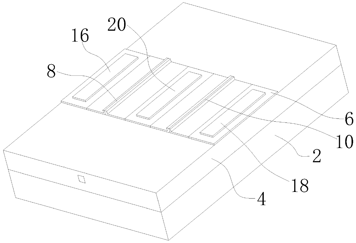
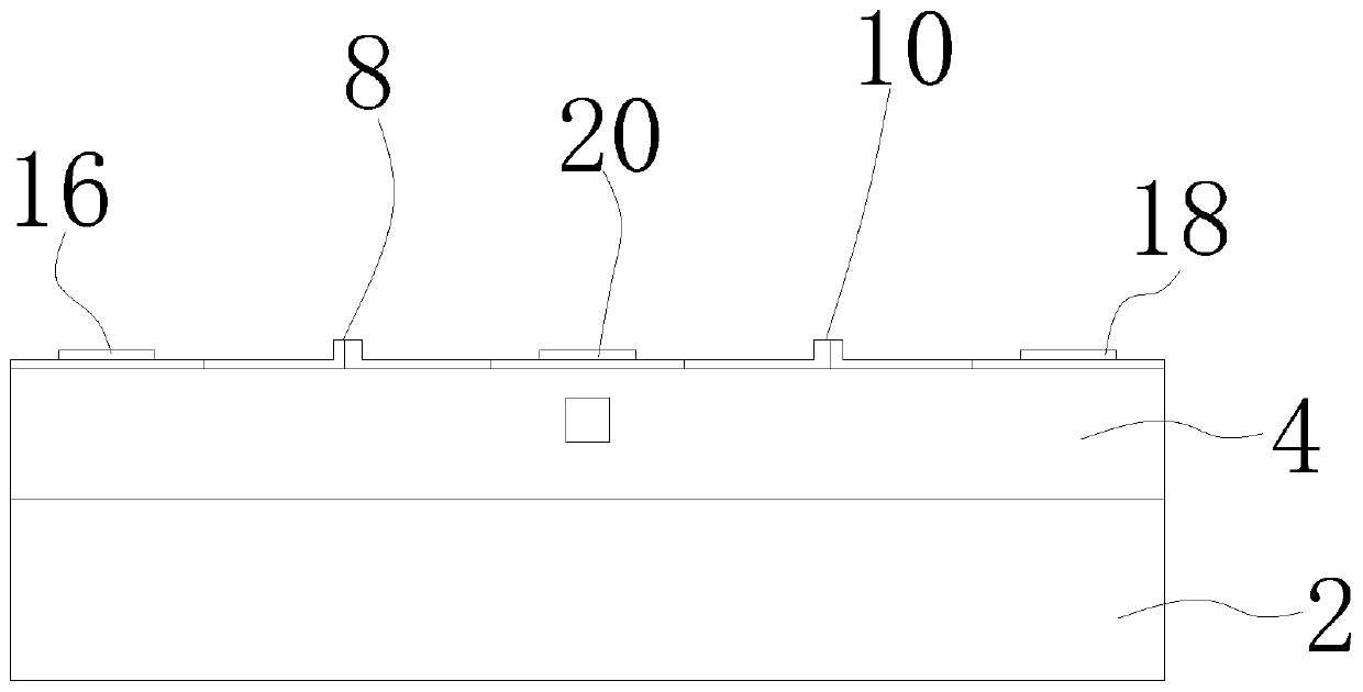
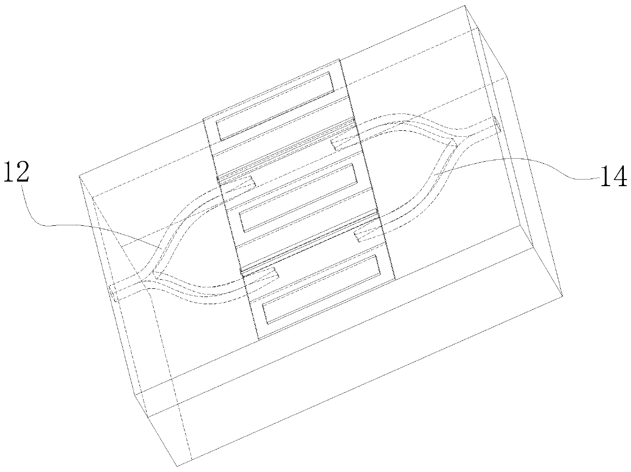
[0027] This embodiment discloses an integrated electro-optic modulator, refer to Figure 1~4 As shown, the integrated electro-optic modulator has a substrate 2, SiO 2 layer 4 and Si layer 6, the electro-optic modulator heterogeneously integrates a PLC waveguide splitter, a PLC waveguide combiner and a pair of silicon waveguide phase shift arms.

[0028] Specifically, a silicon waveguide is formed on the Si layer 6 by etching, and then a first silicon waveguide phase shift arm 8 with a PN structure or a PIN structure is formed by doping; and a silicon waveguide is formed on the Si layer 6 by etching, and then The second silicon waveguide phase shift arm 10 of a PN structure or a PIN structure is formed by doping.

[0029] The above SiO 2 Layer 4 is provided with a PLC waveguide splitter 12 and a PLC waveguide combiner 14 . Here, the PLC waveguide splitter is a splitter that uses PLC waveguides to transmit optical signals, and the PLC waveguide combiner is a combiner that use...


PUM


Abstract

The invention discloses an integrated electro-optical modulator, comprising a SiO2 layer and a Si layer which are arranged in a stacked mode. A first silicon waveguide phase shift arm and a second silicon waveguide phase shift arm are arranged on the Si layer, and a PLC waveguide shunt and a combiner are arranged in the SiO2 layer. Two branches of the PLC waveguide splitter are respectively communicated with the first silicon waveguide phase shift arm light path and the second silicon waveguide phase shift arm light path based on evanescent wave coupling, and two branches of the PLC waveguidecombiner are respectively communicated with the first silicon waveguide phase shift arm light path and the second silicon waveguide phase shift arm light path based on evanescent wave coupling. The invention discloses an integrated electro-optical modulator. The PLC waveguide splitter / combiner is matched with the silicon waveguide phase shift arm to realize electro-optical modulation, so that high-speed electro-optical modulation is realized by utilizing the silicon waveguide phase shift arm, and low-loss direct coupling of the modulator and the optical fiber is realized by utilizing the characteristic that the PLC waveguide device is matched with a single-mode optical fiber mode field. The problems that according to traditional silicon-based electro-optical modulation, due to the fact that mismatch between a silicon waveguide and a single-mode optical fiber mode field is large, a mode spot converter or a vertical coupling grating of a complex structure needs to be arranged to achieveoptical fiber coupling, and coupling loss is large are solved.

Description

technical field [0001] The invention relates to the technical field of integrated electro-optic modulators, in particular to an integrated electro-optic modulator. Background technique [0002] The integrated optical transceiver chip is the core device in the optical transceiver module. It has important and extensive applications in optical communication and data interconnection systems. The integrated optical transceiver chip technology is also an urgent breakthrough for my country to break the monopoly of foreign technology and realize the autonomy of core chips. key technologies. The silicon-based integrated optical transceiver chip supports 100G / 400G and even higher-speed transmission, and supports COB packaging technology, which has great advantages in terms of integration and cost. [0003] The electro-optic modulator is the most critical device unit in the integrated optical transceiver chip. The current mainstream technical solutions are: (1) LiNbO 3 Electro-optic m...

Claims


Application Information

Patent Timeline
Patent Type & Authority Applications(China)
IPC IPC(8): G02F1/035G02F1/025G02B6/125
CPCG02F1/035G02F1/025G02B6/125G02B2006/12142
Inventor 王皓朱宇陈奔施伟明吴邦嘉沈笑寒张拥建洪小刚邢园园吴有强
Owner HENGTONG ROCKLEY TECHNOLOGY CO LTD
Why Eureka
Try Eureka