

Direct-current solid-state transformer with bipolar output voltage self-balancing capability
A technology of solid-state transformer and output voltage, which is applied in the direction of output power conversion device, adjustment of electric variable, high-efficiency power electronic conversion, etc. It can solve the problems of increasing system cost and achieve the effect of cost saving
- Summary
- Abstract
- Description
- Claims
- Application Information
AI Technical Summary
Problems solved by technology
Method used
Image

Examples
specific Embodiment approach 1
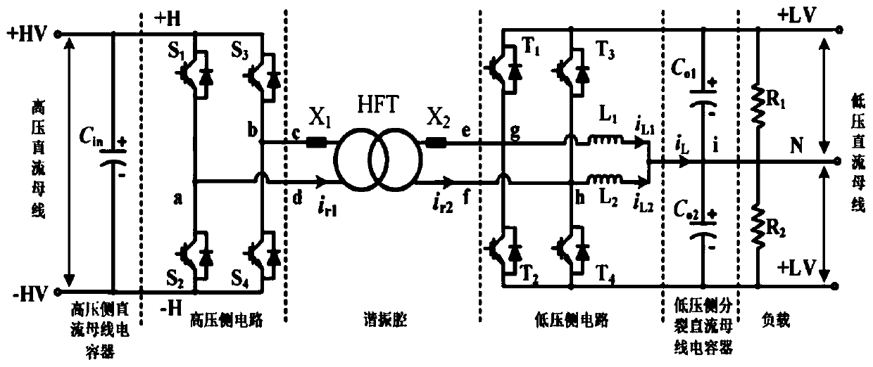
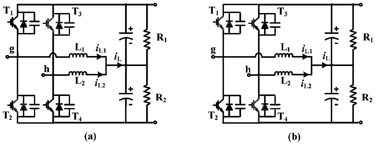
[0020] Specific implementation mode one: as figure 1 As shown, this embodiment discloses a DC solid-state transformer with bipolar output voltage self-balancing capability, including a high-voltage DC bus, a high-voltage side DC bus capacitor, a high-voltage side circuit, a resonant cavity, a low-voltage side circuit, and a low-voltage side split DC bus. A capacitor, a load and a low-voltage DC bus, the high-voltage side circuit includes a first bridge arm and a second bridge arm, and the low-voltage side circuit includes a third bridge arm, a fourth bridge arm, and a balance inductor L 1 and balanced inductance L 2 ;
[0021] The high-voltage side DC bus capacitor, the first bridge arm and the second bridge arm are connected in parallel between the positive pole and the negative pole of the high-voltage DC bus bar, and the low-voltage side splits the DC bus capacitor, load, third bridge arm and fourth bridge arm The bridge arms are all connected in parallel between the posi...
specific Embodiment approach
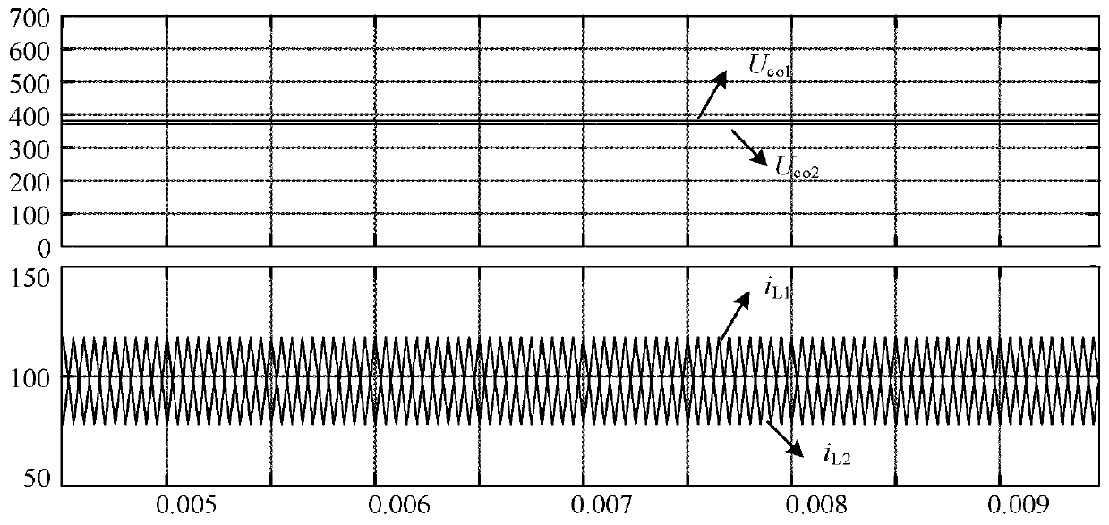
[0034] Taking a 1kV / ±375V DC solid-state transformer with bipolar output voltage self-balancing capability as an example to further illustrate the specific implementation of the present invention: the DC input voltage on the high voltage side is 1kV, and the bipolar output voltage on the low voltage side is ±375V. The pole rated output is 75kW each. As preferred, with load R 1 open circuit, load R 2 It is equal to 1.875 ohms to design this case, at this time, it flows through the balance inductance L 1 with balanced inductance L 2 The inductor current is 100A. Preferably, the inductor current ripple is ±20%, the switching frequency is 10kHz, and the resulting balanced inductance L is designed 1 with balanced inductance L 2 The value is about 88.5μH. Get the simulated waveform as image 3 As shown, the current on the inductor changes between 80 and 120A, and the voltage of the two split capacitors remains balanced. At this time, the simulation waveforms of the output vol...
PUM
 Abstract
Description
Claims
Application Information