Automatic addressing laser scanning electrode structure, control method and manufacturing method

A technology of laser scanning and automatic addressing, applied in the field of microelectronics and optics

Active Publication Date: 2020-06-16
SOUTH UNIVERSITY OF SCIENCE AND TECHNOLOGY OF CHINA +1
View PDF6 Cites 1 Cited by
  • Summary
  • Abstract
  • Description
  • Claims
  • Application Information

AI Technical Summary

Problems solved by technology

In the existing technology, the technical problem of how to realize the

Method used


Image

  • Automatic addressing laser scanning electrode structure, control method and manufacturing method
  • Automatic addressing laser scanning electrode structure, control method and manufacturing method
  • Automatic addressing laser scanning electrode structure, control method and manufacturing method

Examples


Embodiment 1

[0087] Example 1:

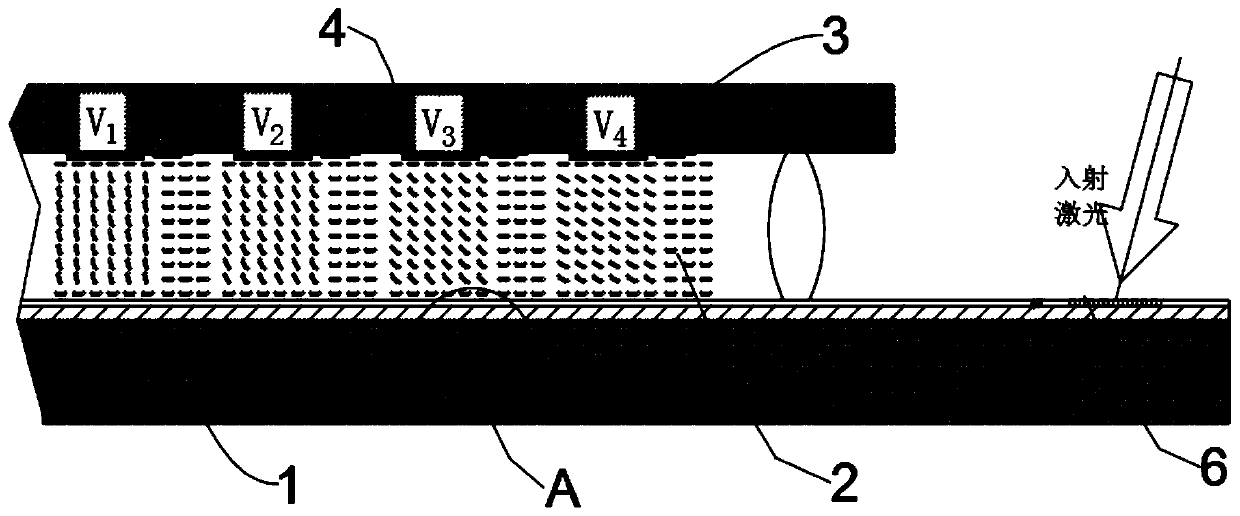
[0088] Such as figure 1 As shown, a self-addressing laser scanning electrode structure includes a conductive substrate 1 with a waveguide structure, a liquid crystal layer 2 is arranged above the conductive substrate, an electrode control array panel 3 is arranged above the liquid crystal layer, and the electrode control Several transparent and conductive driving electrodes 4 are arranged on the array panel, so that the switching state and applied voltage of each driving electrode can be independently controlled, and the driving electrodes are respectively connected to a master controller.

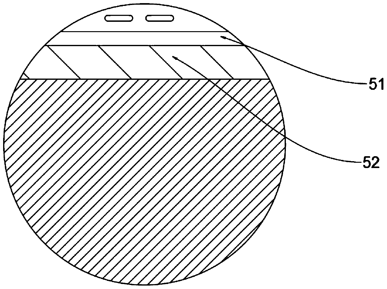
[0089] It includes a light guiding layer 5, the light guiding layer includes a first layer structure 51 and a second layer structure 52, the refractive index of the first layer structure is higher than the refractive index of the second layer structure.

[0090] Preferably, a grating film coupling device 6 is arranged on the light guiding layer 5, and the incident lase...

Embodiment 2

[0097] Such as Figure 4 , based on the device in embodiment 1, we provide a kind of automatic addressing laser scanning electrode control method in embodiment 2, comprising the following steps:

[0098] (1) Determine the preset propagation trajectory of the laser;

[0099] (2) Determine the coordinates of the driving electrodes that need to be driven according to the preset propagation trajectory of the laser;

[0100] (3) Controlling the voltage of the driving electrodes so that the laser light entering the liquid crystal layer is deflected according to a preset propagation track.

[0101] Preferably, the following steps are also included:

[0102] (4) Control the coordinates and directions of the driving electrodes according to the preset laser scanning requirement range, and then realize the laser scanning in the preset angle range.

[0103] Preferably, in said step (1), the following steps are included:

[0104] (11) Equivalent the laser preset propagation trajectory ...

Embodiment 3

[0125] Through the method in this embodiment 2, we provide a kind of embodiment 3, to specifically regulate the laser deflection direction:

[0126] In step (2), a combination of several micro-biasing units of the same shape is used to control the laser deflection according to a preset trajectory, including the following steps:

[0127] Set the angle between the incident straight side and the outgoing straight side for each micro-bias unit

[0128] Set to use the same voltage to control the micro-bias control unit;

[0129] According to the set voltage value and angle Calculate the angle at which each micro-bias unit can adjust the laser deflection, so as to determine the number N of micro-bias units required to achieve laser deflection;

[0130] The center of the circumscribed circle of the triangle formed by the incident side and the outgoing side of each micro-deflection unit is equidistantly set on the equivalent circular arc of the preset laser deflection track, so a...


PUM

PropertyMeasurementUnit
Thicknessaaaaaaaaaa

Abstract

The invention provides an automatic addressing laser scanning electrode structure comprising a substrate. A liquid crystal layer is arranged above the substrate, an electrode control array panel is arranged above the liquid crystal layer, and a plurality of conductive driving electrodes are arranged on the electrode control array panel, so that the on-off state and the applied voltage of each driving electrode can be independently controlled; and the driving electrodes are respectively connected with a master controller. The invention provides an effective laser deflection technical scheme capable of being regulated and controlled in real time, pixel-level control can be set for the electrode control array, high-precision pixel control is achieved, so that the multifunctional liquid crystal laser scanning device capable of regulating and controlling the deflection angle at any time is achieved.

Description

technical field [0001] The invention relates to the fields of microelectronics and optics, in particular to an automatic addressing laser scanning electrode structure, a control method and a manufacturing method. Background technique [0002] In the design of the liquid crystal waveguide laser scanning device, the design of the deflection electrode has a great influence on the final performance of the device, especially the size of the scanning angle. In this type of device, the refractive index of the liquid crystal is regulated by the driving electrode. By designing the shape of the driving electrode (such as a triangle), the liquid crystal layer of the part driven by the electrode forms a refractive index difference with the surrounding liquid crystal that is not driven by voltage and is in contact with the designed electrode. corresponding to the shape. When the laser light transmitted in the light guide layer passes through this region, it is deflected at a certain ang...

Claims


Application Information

Patent Timeline
IPC IPC(8): G02F1/1343G02F1/1335G02F1/135G02F1/1362
CPCG02F1/134309G02F1/133504G02F1/135G02F1/1362
Inventor 邱成峰娄飞刘红均孙小卫刘召军程鑫庹勇
Owner SOUTH UNIVERSITY OF SCIENCE AND TECHNOLOGY OF CHINA
Why Eureka
Try Eureka