
Field effect transistor, preparation method and electronic equipment

A technology for field effect transistors and electronic devices, applied in the field of electronics, can solve problems such as the need for improvement of electronic devices

Pending Publication Date: 2020-06-23
BYD SEMICON CO LTD
View PDF7 Cites 2 Cited by
  • Summary
  • Abstract
  • Description
  • Claims
  • Application Information

AI Technical Summary

Problems solved by technology

[0003]However, the current SiCMOS tube and its preparation method and electronic equipment still need to be improved

Method used


Image

  • Field effect transistor, preparation method and electronic equipment
  • Field effect transistor, preparation method and electronic equipment
  • Field effect transistor, preparation method and electronic equipment

Examples


Embodiment Construction

[0018] Embodiments of the present invention are described in detail below, examples of which are shown in the drawings, wherein the same or similar reference numerals designate the same or similar elements or elements having the same or similar functions throughout. The embodiments described below by referring to the figures are exemplary only for explaining the present invention and should not be construed as limiting the present invention.

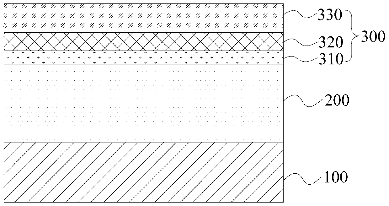
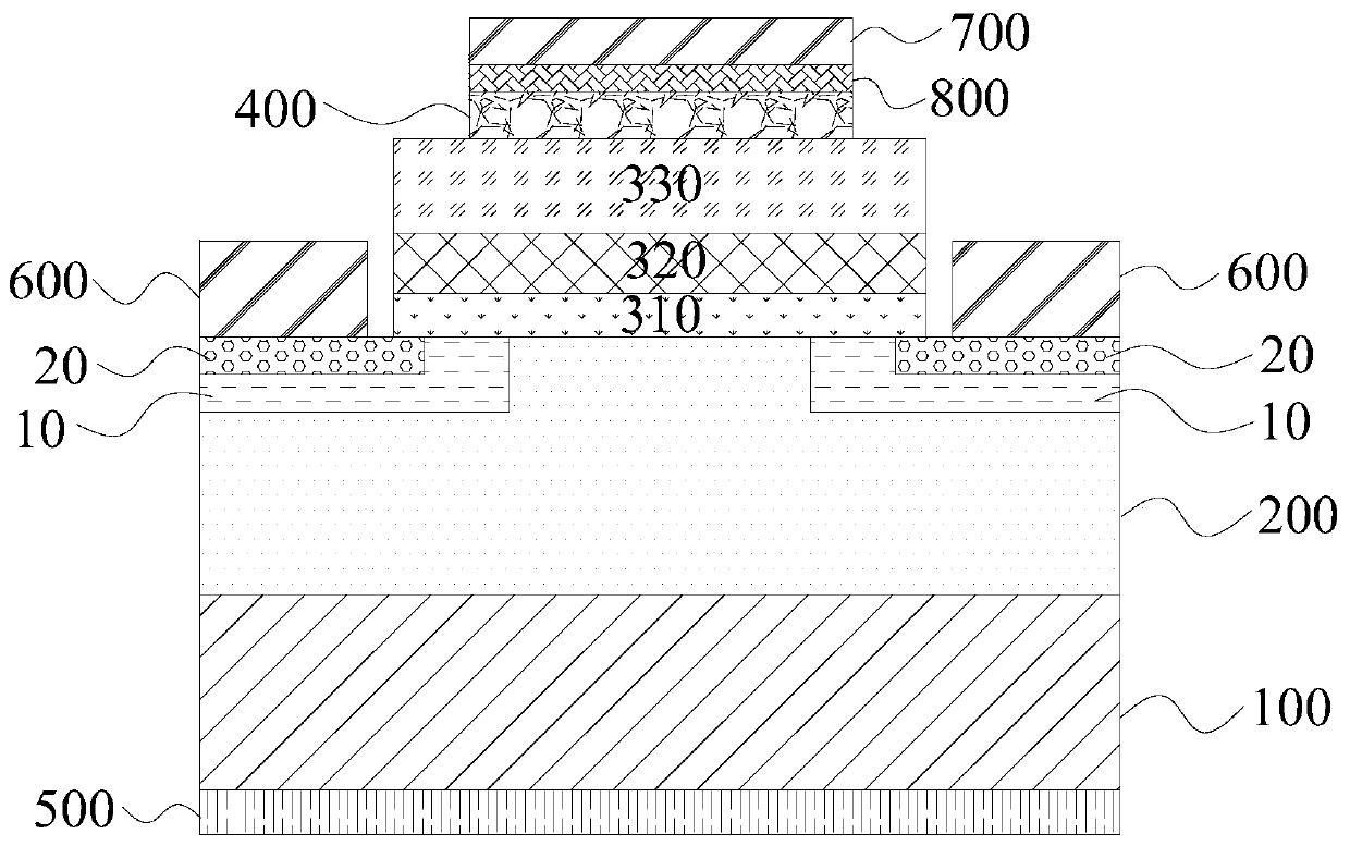
[0019] In one aspect of the invention, the invention provides a field effect transistor. According to an embodiment of the present invention, refer to figure 1 , the field effect transistor includes a SiC substrate 100 , a SiC epitaxial layer 200 and a gate oxide structure 300 which are sequentially stacked. Wherein, the gate oxide structure 300 includes a transition layer 310, a barrier layer 320 and an oxide layer 330 which are sequentially stacked. All materials are SiO 2 , the thickness of the transition layer 310 is smaller than ...


PUM

PropertyMeasurementUnit
Thicknessaaaaaaaaaa
Doping concentrationaaaaaaaaaa

Abstract

The invention discloses a field effect transistor, a preparation method and electronic equipment. The field effect transistor comprises a SiC substrate, a SiC epitaxial layer and a gate oxide structure which are sequentially arranged in a stacked mode, wherein the gate oxide structure comprises a transition layer, a barrier layer and an oxide layer which are sequentially stacked, the transition layer is arranged on the side, which is away from the SiC substrate, of the SiC epitaxial layer, the transition layer and the oxide layer are both made of SiO2, and the thickness of the transition layeris less than that of the oxide layer. Therefore, the interface between the gate oxide structure and the SiC epitaxial layer of the field effect transistor has a good interface state, so that the interface between the gate oxide structure and the SiC epitaxial layer has high mobility, the gate oxide structure has high reliability, and the field effect transistor is enabled to have good use performance.

Description

technical field [0001] The invention relates to the field of electronics, in particular to a field effect transistor, a preparation method, and an electronic device. Background technique [0002] SiC is a typical representative of the third-generation wide bandgap semiconductor material, which has the characteristics of wide bandgap, high thermal conductivity, high breakdown electric field strength, high saturation mobility, and strong radiation resistance. Metal-oxide-semiconductor field-effect transistors (hereinafter referred to as SiCMOS transistors) based on SiC materials have the characteristics of high breakdown electric field, fast switching speed, low switching loss, strong thermal conductivity, and radiation resistance. They are suitable for high-voltage, high-frequency, high-speed, high power applications. [0003] However, the current SiCMOS tube, its preparation method and electronic equipment still need to be improved. Contents of the invention [0004] The...

Claims


Application Information

Patent Timeline
IPC IPC(8): H01L29/423H01L29/51H01L29/78H01L21/336H01L21/28
CPCH01L29/7827H01L29/66068H01L29/401H01L29/42364H01L29/511
Inventor 曹群肖秀光
Owner BYD SEMICON CO LTD
Learn More