
Memory and forming method thereof, and memory cell array and driving method thereof

A storage unit, memory technology, applied in static memory, digital memory information, information storage, etc., can solve problems such as poor performance of split-gate flash memory

Pending Publication Date: 2020-06-26
SHANGHAI HUAHONG GRACE SEMICON MFG CORP
View PDF0 Cites 0 Cited by
  • Summary
  • Abstract
  • Description
  • Claims
  • Application Information

AI Technical Summary

Problems solved by technology

[0004] However, the performance of existing split-gate flash memory is poor

Method used


Image

  • Memory and forming method thereof, and memory cell array and driving method thereof
  • Memory and forming method thereof, and memory cell array and driving method thereof
  • Memory and forming method thereof, and memory cell array and driving method thereof

Examples


Embodiment Construction

[0045] As mentioned in the background, the performance of flash memory is poor.

[0046] The reasons for the problems are described below in conjunction with the accompanying drawings.

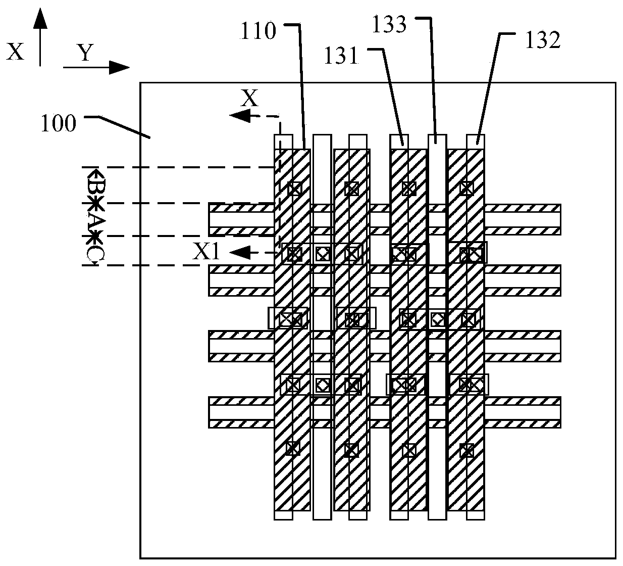
[0047] figure 1 is a schematic diagram of a memory cell array.

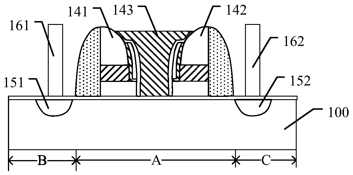
[0048] An array of memory cells, see figure 1 , comprising: a semiconductor substrate 100, the semiconductor substrate 100 comprising: several parallel and discrete active regions 110 arranged in parallel along the second direction Y, and an isolation structure surrounding the active regions 110 (not shown in the figure) , the active regions 110 extend along the first direction X, and each of the active regions 110 in the first direction X includes several memory cell regions, and each memory cell region includes: a storage region A and a storage region located in the storage region Source region B and drain region C on both sides of A; several source regions, and one source region in the source region B; several drain regions...


PUM


Abstract

Provided are a memory and a forming method thereof, a memory cell array and a driving method thereof. The memory comprises a substrate which includes a first storage region and a second storage regionadjacent to and separated from each other, a source region which is positioned in the substrate between the first storage region and the second storage region, a first drain region and a second drainregion which are positioned in the substrate on the two sides of the first storage region and the second storage region, a first storage structure which is located on the first storage region and comprises a first storage unit, a second storage unit and a first word line gate located between the first storage unit and the second storage unit, and a second storage structure which is located on thesecond storage region and comprises a third storage unit, a fourth storage unit and a second word line gate located between the third storage unit and the fourth storage unit. The performance of thememory is improved.

Description

technical field [0001] The invention relates to the field of semiconductor manufacturing, in particular to a memory and its forming method, a memory cell array and its driving method. Background technique [0002] In the current semiconductor industry, integrated circuit products can be mainly divided into three types: analog circuits, digital circuits, and digital / analog hybrid circuits. Among them, memory is an important type of digital circuits. In memory, the development of flash memory (flash memory, referred to as flash memory) is particularly rapid in recent years. The main feature of flash memory is that it can keep storing information for a long time without power on, and has the advantages of high integration, fast storage speed, easy erasing and rewriting, etc. Therefore, it has been widely used in many fields such as microcomputers and automatic control. Wide range of applications. [0003] Flash memory is classified into two types: stack gate flash memory and ...

Claims


Application Information

Patent Timeline
IPC IPC(8): H01L27/11517H01L27/11519H01L27/11521G11C11/4063
CPCG11C11/4063H10B41/00H10B41/10H10B41/30H01L29/42328H01L29/40114G11C5/025H01L29/66825H01L29/788
Inventor 于涛
Owner SHANGHAI HUAHONG GRACE SEMICON MFG CORP
Features
  • Generate Ideas
  • Intellectual Property
  • Life Sciences
  • Materials
  • Tech Scout
  • Unparalleled Data Quality
  • Higher Quality Content
  • 60% Fewer Hallucinations
Learn More