
Novel optical mask plate with different light transmission properties

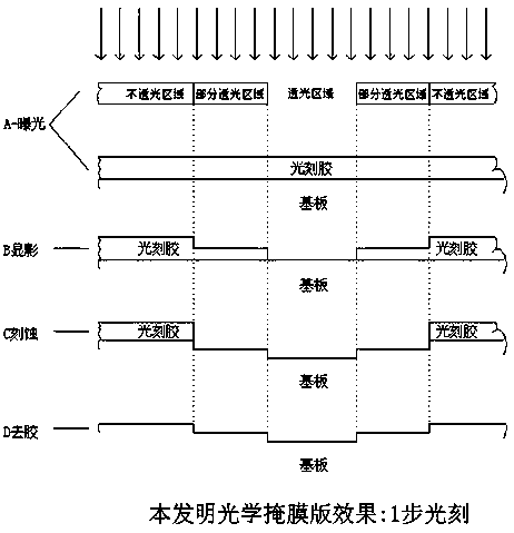
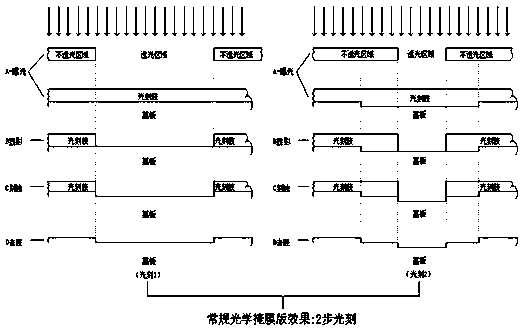
An optical mask and light transmittance technology, applied in the field of lithography, can solve the problems of cumbersome preparation process, reduce lithography steps, achieve the effect of size and height, and meet the requirements of lithography masks

Inactive Publication Date: 2020-07-03
JUCAN PHOTOELECTRIC TECH (SUQIAN) CO LTD
View PDF19 Cites 3 Cited by
  • Summary
  • Abstract
  • Description
  • Claims
  • Application Information

AI Technical Summary

Problems solved by technology

[0004] In the actual use of photolithography, many processes require photoresist to form multi-step topography. When using conventional optical masks for photolithography, step topography must be formed through multiple exposures, and the preparation process is cumbersome.

Method used


Image

  • Novel optical mask plate with different light transmission properties
  • Novel optical mask plate with different light transmission properties
  • Novel optical mask plate with different light transmission properties

Examples


Embodiment 1

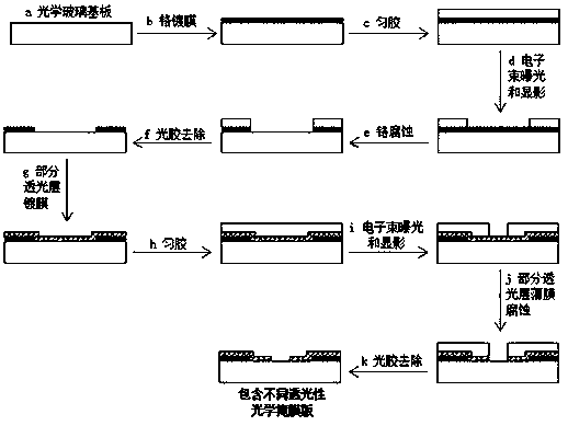
[0036] A novel optical mask comprising different light transmittances, the preparation method of which comprises the following steps:

[0037] a. Select optical glass with high transmittance in the ultraviolet band as the substrate of the optical mask;

[0038] b. Coating a layer of chromium metal film on the surface of the glass substrate;

[0039] c. Uniformly coat a layer of photoresist on the glass substrate coated with chrome film;

[0040] d. Set the photoresist in the pattern area by electron beam exposure to make it react, and then develop it with a developer to finally form a glass substrate with a photoresist pattern;

[0041] e. Soak the etching solution to remove the chromium film in the area not covered by the photoresist, and keep the rest;

[0042] f. Remove the remaining photoresist to form a glass substrate with fully transparent and fully blocked light design graphics;

[0043] g. Continue to coat a layer of partially light-transmitting film on the glass s...

Embodiment 2

[0061] A novel optical mask comprising different light transmittances, the preparation method of which comprises the following steps:

[0062] a. Select optical glass with high transmittance in the ultraviolet band as the substrate of the optical mask;

[0063] b. Coating a layer of chromium metal film on the surface of the glass substrate;

[0064] c. Uniformly coat a layer of photoresist on the glass substrate coated with chrome film;

[0065] d. Set the photoresist in the pattern area by electron beam exposure to make it react, and then develop it with a developer to finally form a glass substrate with a photoresist pattern;

[0066] e. Soak the etching solution to remove the chromium film in the area not covered by the photoresist, and keep the rest;

[0067] f. Remove the remaining photoresist to form a glass substrate with fully transparent and fully blocked light design graphics;

[0068] g. Continue to coat a layer of partially light-transmitting film on the glass s...

Embodiment 3

[0082] A novel optical mask comprising different light transmittances, the preparation method of which comprises the following steps:

[0083] a. Select optical glass with high transmittance in the ultraviolet band as the substrate of the optical mask;

[0084] b. Coating a layer of chromium metal film on the surface of the glass substrate;

[0085] c. Uniformly coat a layer of photoresist on the glass substrate coated with chrome film;

[0086] d. Set the photoresist in the pattern area by electron beam exposure to make it react, and then develop it with a developer to finally form a glass substrate with a photoresist pattern;

[0087] e. Soak the etching solution to remove the chromium film in the area not covered by the photoresist, and keep the rest;

[0088] f. Remove the remaining photoresist to form a glass substrate with fully transparent and fully blocked light design graphics;

[0089] g. Continue to coat a layer of partially light-transmitting film on the glass s...


PUM

PropertyMeasurementUnit
thicknessaaaaaaaaaa
thicknessaaaaaaaaaa
thicknessaaaaaaaaaa

Abstract

The invention relates to the technical field of photoetching, particularly to a novel optical mask plate with different light transmittances. The preparation method of the novel optical mask plate comprises the following steps: a, selecting a substrate; b, plating the surface of the glass substrate with a chromium metal film layer on; c, coating the chromium film with a photoresist; d, exposing the photoresist in a set pattern area through an electron beam; e, soaking in an etching solution; f, removing the remaining photoresist; g, plating the glass substrate with a partial light-transmittingfilm; h, uniformly coating the partial light-transmitting film with a photoresist; i, exposing the photoresist in the set pattern area through an electron beam; j, carrying out etching solution soaking or dry etching; and k, removing the remaining photoresist to form a novel optical mask plate. The invention provides a novel optical mask plate with different light transmission properties, photoresist patterns with steps with different heights can be used manufactured by one-time photoetching according to actual requirements, photoetching steps can be ereduced, photoetching mask requirements are met, and the method can be further popularized in actual industrial production.

Description

technical field [0001] The invention relates to the technical field of photolithography, in particular to a novel optical mask with different light transmittances. Background technique [0002] Photolithography is a major process in the production of planar transistors and integrated circuits. Photolithography technology refers to the technology of transferring the pattern on the photoresist plate to the substrate under the action of light with the help of photoresist. The optical reticle is a structure in which various functional patterns are made on the film, plastic or glass substrate material and precisely positioned for selective exposure of the photoresist coating. Masks are widely used, and masks are required in fields involving photolithography, such as IC (Integrated Circuit, integrated circuit), FPD (Flat Panel Display, flat panel display), PCB (Printed Circuit Boards, printed circuit board), MEMS (Micro Electro Mechanical Systems, Micro Electro Mechanical System...

Claims


Application Information

Patent Timeline
Patent Type & Authority Applications(China)
IPC IPC(8): G03F1/88
CPCG03F1/88
Inventor 张振刘佳擎
Owner JUCAN PHOTOELECTRIC TECH (SUQIAN) CO LTD
Learn More