
Array substrate and display panel

A technology of array substrates and base substrates, which is applied in the fields of instruments, electrical digital data processing, electrical components, etc., and can solve problems such as the complexity of the array substrate process

Inactive Publication Date: 2020-07-07
WUHAN CHINA STAR OPTOELECTRONICS TECH CO LTD
View PDF3 Cites 5 Cited by
  • Summary
  • Abstract
  • Description
  • Claims
  • Application Information

AI Technical Summary

Problems solved by technology

Integrating photosensitive sensors into the screen to realize full-screen fingerprint recognition can greatly improve user experience, but the integrated array substrate process will become complicated

Method used


Image

  • Array substrate and display panel
  • Array substrate and display panel
  • Array substrate and display panel

Examples


Embodiment Construction

[0036] In order to better understand the content of the present invention, the present invention will be further described through specific examples below, but the implementation and protection scope of the present invention are not limited thereto.

[0037] The following description of the embodiments refers to the accompanying drawings to illustrate specific embodiments in which the invention may be practiced. The directional terms mentioned in the present invention, such as "up", "down", "front", "back", "left", "right", "top", "bottom", etc., are only for reference to the attached drawings. direction. Therefore, the directional terms used are used to illustrate and understand the present invention, but not to limit the present invention.

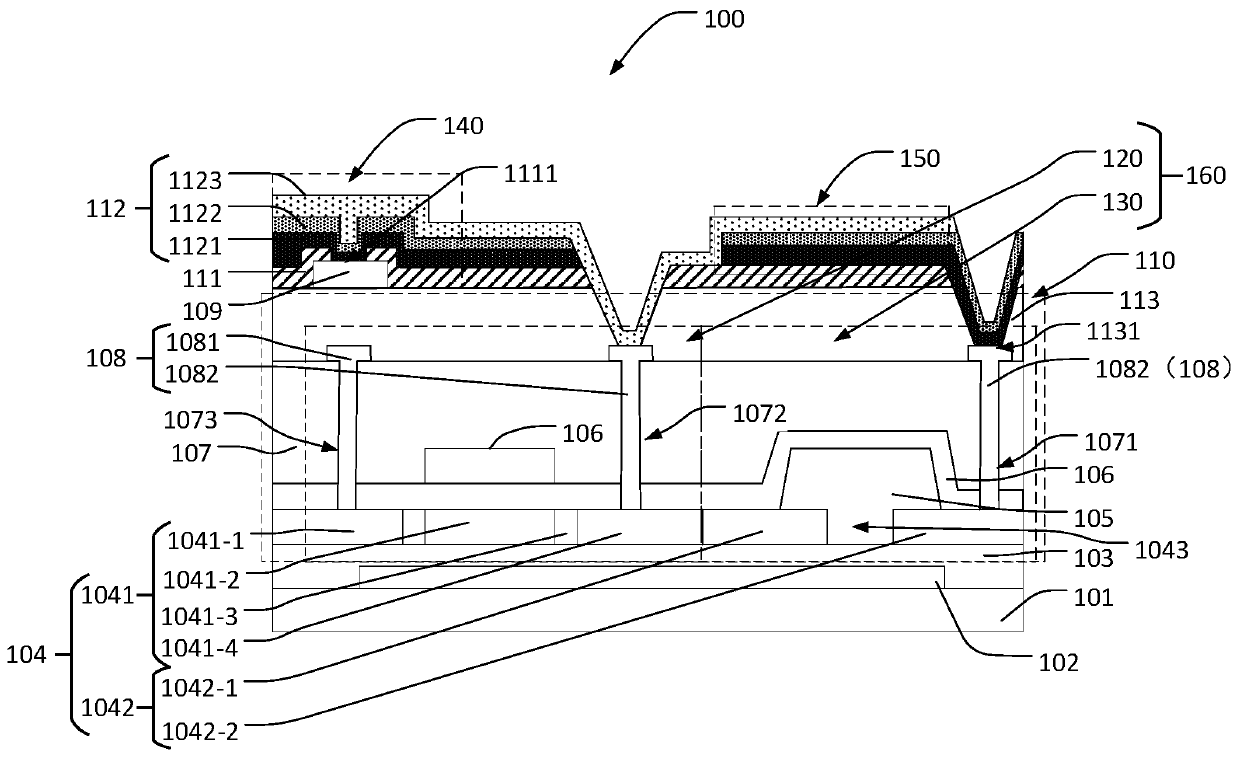
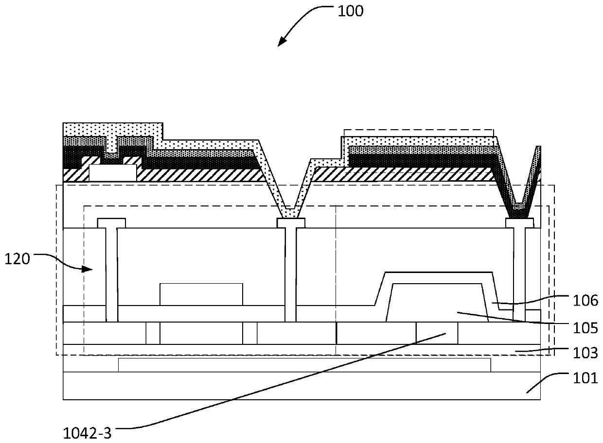
[0038] The invention provides an array substrate, comprising: a base substrate, a thin film transistor layer and a fingerprint recognition component.

[0039] The thin film transistor layer is arranged on the base substrate; the finger...


PUM


Abstract

The invention provides an array substrate and a display panel. The array substrate comprises a substrate body, a thin film transistor layer and a fingerprint recognition assembly. According to the invention, the switching element and the fingerprint identification element of the fingerprint identification assembly are horizontally arranged in the thin film transistor layer, the fingerprint identification element and the switching element can be prepared together when the thin film transistor layer is prepared, the thickness of the panel can be reduced, and the structure is simple and not complex. Specifically, when the first semiconductor and the second semiconductor are prepared, after the corresponding patterns are patterned, phosphorane and borane gases can also be introduced to preparethe doped region together, and extra gas does not need to be introduced, so the cost is saved. Compared with a traditional LTPS manufacturing process, only the mask plate needed by the first P+ dopedregion and the mask plate of the photosensitive layer need to be added, and the manufacturing cost is low.

Description

technical field [0001] The invention relates to the field of display technology, in particular to an array substrate and a display panel. Background technique [0002] Fingerprint identification technology has been widely used in small and medium-sized panels, mainly including capacitive, ultrasonic and optical methods. Compared with capacitive and ultrasonic fingerprint recognition technologies, optical fingerprint recognition has good stability, strong antistatic ability, good penetration ability and low cost. Optical fingerprint recognition technology uses the principle of refraction and reflection of light. When the light is irradiated on the finger, it is received by the photosensitive sensor after being reflected by the finger. After receiving the photosensitive sensor, the optical signal can be converted into an electrical signal for reading. Due to the different light reflections of fingerprint valleys and ridges, the reflected light intensity received by the sensor...

Claims


Application Information

Patent Timeline
Patent Type & Authority Applications(China)
IPC IPC(8): H01L27/12G02F1/1333G02F1/1362G02F1/1368G06F3/044G06K9/00
CPCH01L27/1214H01L27/1255G02F1/136286G02F1/1368G02F1/13338G06F3/044G06V40/1318G06V40/1306
Inventor 李治福肖军城艾飞宋继越
Owner WUHAN CHINA STAR OPTOELECTRONICS TECH CO LTD
Learn More