Semiconductor substrate and method for preparing same
一种半导体、基底的技术,应用在半导体基底及其制备领域
- Summary
- Abstract
- Description
- Claims
- Application Information
AI Technical Summary
Problems solved by technology
Method used
Image

Examples
preparation example Construction
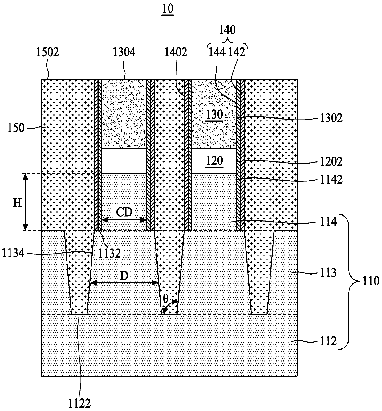
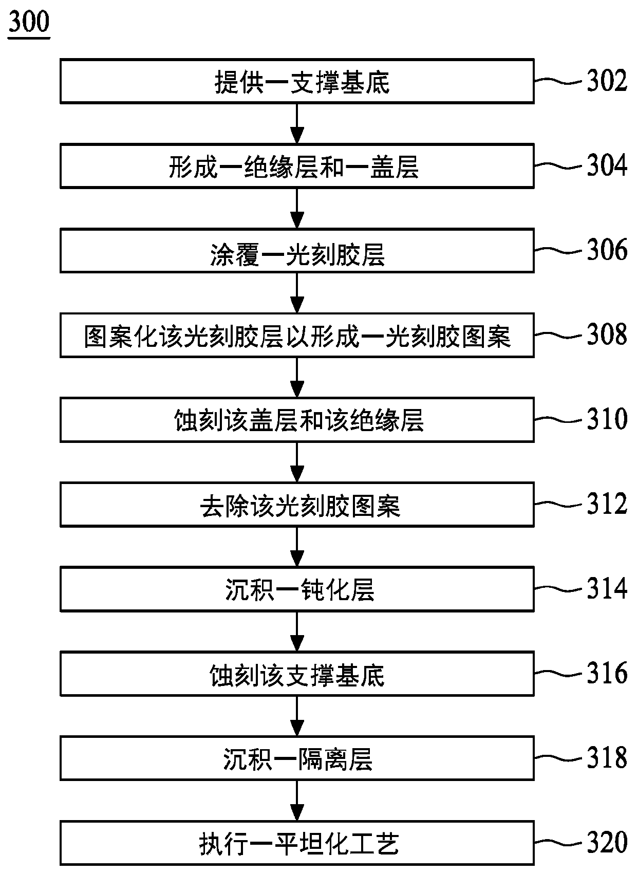
[0081] figure 2 is a method 300 of fabricating a semiconductor substrate 10 illustrating some embodiments of the present disclosure. Figure 3 to Figure 10 are various fabrication stages of a method 300 of fabricating semiconductor structure 10 illustrating some embodiments of the present disclosure. Figure 3 to Figure 11 The various stages of figure 2 Schematic illustration of the manufacturing process. In the follow-up instructions, Figure 3 to Figure 11 The manufacturing steps shown in the corresponding reference figure 2 manufacturing steps in .
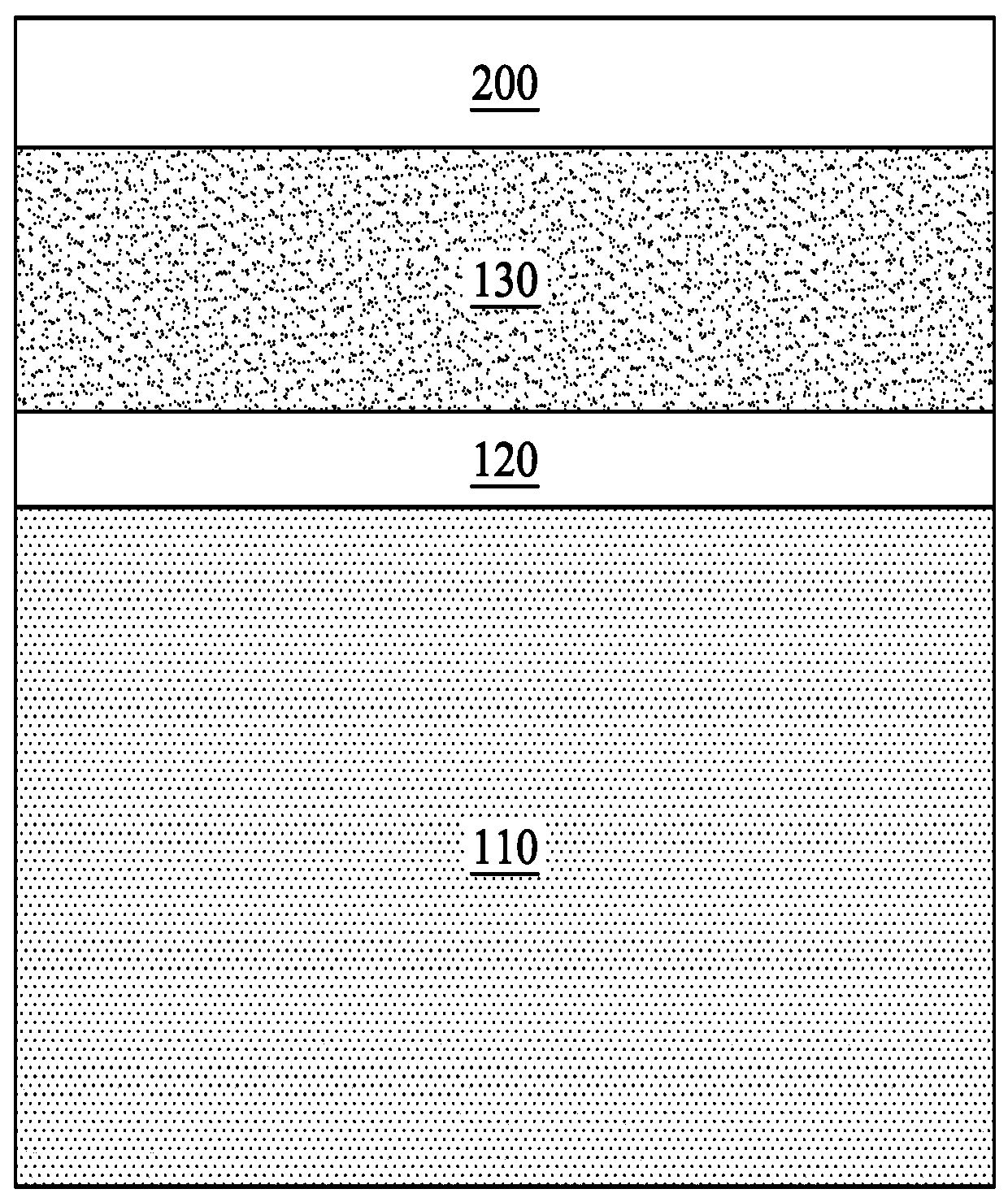
[0082] refer to image 3 ,according to figure 2 In step 302, a support base 110 is provided. In some embodiments, the support substrate 110 is a bulk silicon substrate. In some embodiments, suitable materials for the supporting substrate 110 include, but are not limited to, silicon. In some embodiments, the support substrate 110 may be lightly doped single crystal silicon. In some embodiments, the support substrat...
PUM
 Abstract
Description
Claims
Application Information