Packaging method for inhibiting drifting and warping of chip

A packaging method and warping technology, applied in semiconductor/solid-state device manufacturing, electrical components, electrical solid-state devices, etc., can solve problems such as adverse effects of charge carrier mobility, decreased bonding strength of rewiring layers, and impact on chip electrical performance , to achieve the effect of suppressing drift and warpage, suppressing drift and reducing warpage

Active Publication Date: 2020-07-17
GUANGDONG UNIV OF TECH
View PDF7 Cites 1 Cited by
  • Summary
  • Abstract
  • Description
  • Claims
  • Application Information

AI Technical Summary

Problems solved by technology

The drift of the chip will affect the electrical performance of the chip, because after the chip drifts, its I / O will also shift, and then the redistribution layer will be invalid if it is made in the original position; the warping of the chip will cause the redistribution layer (RDL ) Problems such as decrease in binding strength, fracture, etc., have adverse effects on charge carrier mobility

Method used


Image

  • Packaging method for inhibiting drifting and warping of chip
  • Packaging method for inhibiting drifting and warping of chip
  • Packaging method for inhibiting drifting and warping of chip

Examples


no. 1 example

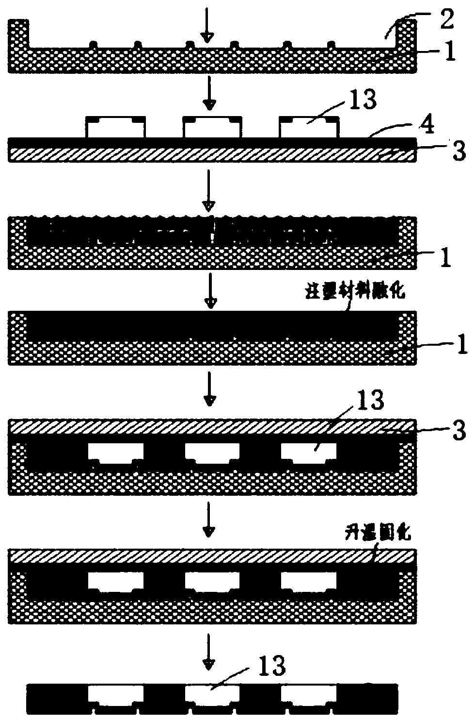
[0053] Such as figure 1 Shown is the first embodiment of the packaging method for suppressing chip drift and warping of the present invention, which includes the following steps:

[0054] S10. Make the first groove 2 on the first rigid carrier 1, install the chips to be packaged on the second rigid carrier 3 covered with the temporary bonding layer 4 according to the required interval and position;

[0055] S20. Spread the injection molding material in the first groove 2 of the first rigid carrier 1, and raise the temperature above the glass transition temperature of the injection molding material to melt the injection molding material, forming a horizontal liquid level in the first groove 2 ;

[0056] S30. Move the second rigid carrier 3 on which the chip to be packaged is installed to the first rigid carrier 1 in such a way that the chip to be packaged faces downward so that the chip to be packaged is inserted into the molten injection molding material, and the second rigid...

Embodiment 2

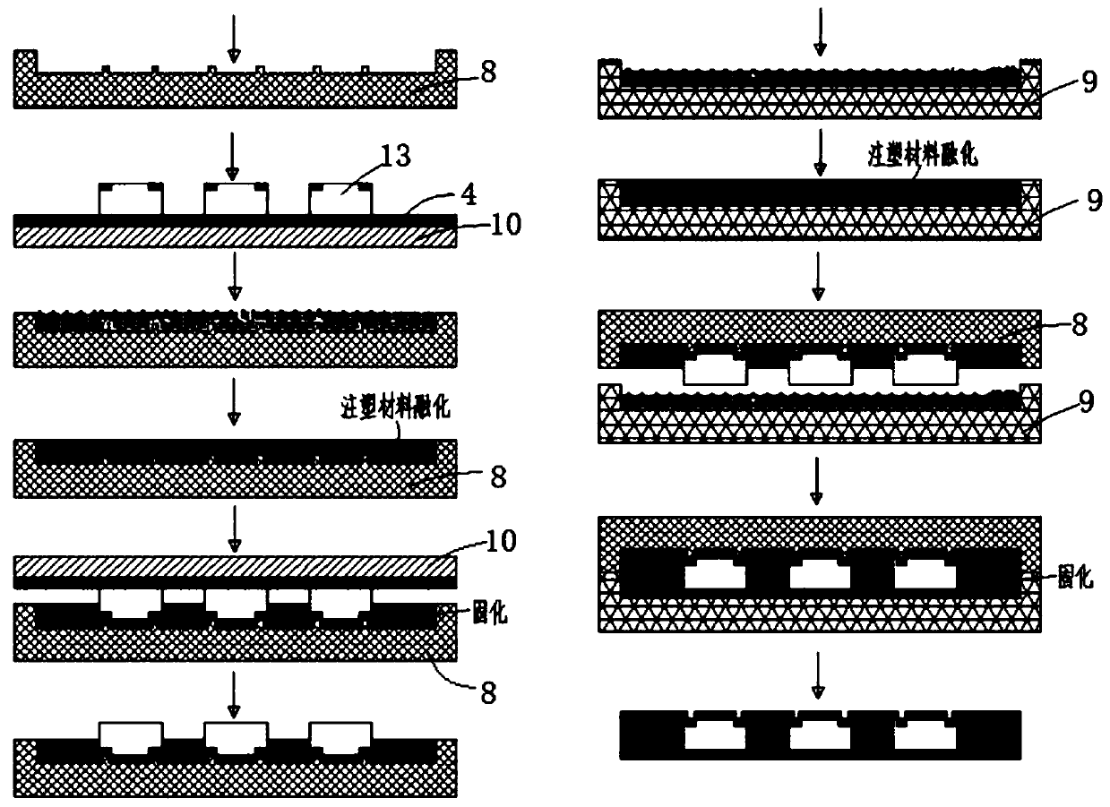
[0067] Such as image 3 Shown is the second embodiment of the package method for suppressing chip drift and warpage of the present invention. When a special curing sequence needs to be implemented, or the chip 13 to be packaged is thick or the viscosity of the injection molding material is too high, so that the chip 13 to be packaged cannot When the molten injection molding material is fully inserted, the method of multiple injection molding packaging can be used, including the following steps:

[0068] S10. Make a third groove with a package shape on the third rigid carrier 8, and make a fourth groove with a package shape on the fourth rigid carrier 9. The depth of the third groove is the same as that of the fourth groove. The sum of the depths of the grooves is equal to the height of the package;

[0069] S20. Install the chips 13 to be packaged on the fifth rigid carrier 10 covered with the temporary bonding layer 4 according to the required interval and position;

[0070...

Embodiment 3

[0080] Such as Figure 4 Shown is the third embodiment of the packaging method for suppressing chip drift and warpage of the present invention, when a special curing sequence is required, or the chip is thick or the viscosity of the injection molding material is too high, so that the chip cannot be completely inserted into the molten injection molding material When the method of multiple injection molding packaging can also be used; when the required final package height is consistent with the height of the chip, the packaging method to suppress chip drift and warpage includes the following steps:

[0081] S10. Make a sixth groove with a package shape on the sixth rigid carrier 11, the depth of the sixth groove is equal to the height of the chips to be packaged 13; the chips to be packaged 13 are installed in the required interval and position On the seventh rigid carrier 12 covered with the temporary bonding layer 4;

[0082] S20. Spread the fifth injection molding material ...


PUM


Abstract

The invention relates to the technical field of electronic processing, more specifically, the present invention relates to a packaging method for inhibiting the drifting and warping of a chip. The method comprises the steps of manufacturing a first groove in a first rigid carrier plate, manufacturing a patterned protrusion at the bottom of the first groove, laying an injection molding material flatly in the first groove and then heating the injection molding material to be molten, then inserting a chip to be packaged into the molten injection molding material in an inverted mode, carrying outthe controllable temperature field type heating curing to obtain a packaged chip obtained after plastic packaging. When a special packaging structure and a curing sequence need to be realized, or under the conditions or requirements of a thicker chip to be packaged or an injection molding material with over-high viscosity and the like, a multi-time inversion method can be adopted to realize the multi-material and multi-sequence injection molding curing. According to the invention, the controllable temperature field type temperature rise and the structural design of the rigid support plate arecombined, so that the controllable curing molding of the multi-layer packaging structure can be realized, the shrinkage force during the curing of the injection molding material and the residual stress of the cured packaging body are regulated and controlled, and the drifting and warping of the chip are reduced.

Description

technical field [0001] The invention relates to the technical field of electronic processing, more specifically, to a packaging method for suppressing chip drift and warpage. Background technique [0002] With the development of microelectronic packaging technology, the chip size is getting smaller and smaller, and the number of transistors is getting higher and higher, and the large board-level fan-out packaging technology has been derived. Fan-Out Panel Level Packaging technology is to package the chip with plastic packaging material first, and then realize the extension of the chip I / O port through metal connection methods such as metal redistribution line layer (RDL). As the substrate area increases and the thickness of the package becomes thinner, previously unknown or insignificant forces affect the yield of the packaged chip. The shrinkage forces generated during curing, which cause chip drift and warpage, respectively. The drift of the chip will affect the electric...

Claims


Application Information

Patent Timeline
Patent Type & Authority Applications(China)
IPC IPC(8): H01L21/56H01L21/67H01L23/13
CPCH01L21/568H01L23/13H01L21/67098
Inventor 杨冠南罗绍根崔成强张昱
Owner GUANGDONG UNIV OF TECH
Why Eureka
Try Eureka