MEMS device and method of manufacturing the same

a technology of a movable member and a manufacturing method, which is applied in the direction of instruments, other domestic objects, optical elements, etc., can solve the problems of difficult to reduce the mirror interval of the micromirror device, and the inability to guide light of a wavelength concerned to an output port, so as to reduce or prevent charge accumulation, suppress the tilt angle of the movable member, and prevent metal film formation

Active Publication Date: 2011-01-20
NIPPON TELEGRAPH & TELEPHONE CORP
View PDF6 Cites 15 Cited by
  • Summary
  • Abstract
  • Description
  • Claims
  • Application Information

AI Technical Summary

Benefits of technology

[0036]According to the present invention, a driving stabilization electrode made of a metal or a semiconductor is provided in contact with the insulating film of the second substrate. This allows to reduce or prevent charge accumulation in the insulating film provided on the surface of the second substrate even when a voltage is applied to the fixed electrodes (driving electrodes) of the MEMS device. It is therefore possible to suppress the phenomenon that the tilt angle of the movable member of the MEMS device changes over time, i.e., drift of the tilt angle.
[0037]According to the present invention, first and second metal films made of the same metal material as that of the driving electrodes and having the same shape are formed to be similar to and smaller than the movable member, and arranged concentrically with the movable member. No metal such as Au is formed on the support members. This enables to suppress drift of the tilt angle of the movable member. Additionally, in the present invention, the movable member having, on its surfaces, the metal films made of the same metal as that of the driving electrodes can be prevented from sticking to the driving electrodes.
[0038]According to the present invention, the silicon base portion existing in the region where the support members and the movable member are formed is etched until the buried oxide layer of the SOI substrate is exposed. A resist pattern having an opening region corresponding to the region with the movable member is formed on the exposed buried oxide layer. The buried oxide layer exposed to the opening region of the resist pattern and the buried oxide layer near the edge of the opening region are removed. A metal film is deposited on the movable member of the SOI substrate using the resist pattern as a mask, thereby preventing metal film formation on the support members. This allows to suppress drift of the tilt angle of the movable member. Additionally, in the present invention, the metal film can be formed while separating the metal film adhered to the side walls of the resist pattern and the metal film deposited on the desired movable member. It is therefore possible to form a metal film having a fine surface shape on the movable member such as a mirror upon stripping (lift-off) of the resist pattern.
[0039]According to the present invention, the silicon base portion and the buried oxide layer of the SOI substrate existing in the region where the support members and the movable member are formed are etched until the SOI layer is exposed. A resist thinner than the silicon base portion is applied onto the exposed SOI layer. A resist pattern is formed by exposing the resist from the side of the SOI layer on the opposite side of the silicon base portion using a portion except the support members as a mask, thereby preventing metal film formation on the support members. This allows to suppress drift of the tilt angle of the movable member. Additionally, in the present invention, a resist pattern that is thinner than the silicon base portion and having a reverse tapered shape can be formed as a mask for metal film formation. The metal film can be formed while separating the metal film adhered to the surface of the resist pattern and the metal film deposited on the surface of the SOI layer. It is therefore possible to form a metal film having a fine surface shape on the movable member such as a mirror upon stripping (lift-off) of the resist pattern.

Problems solved by technology

This makes it impossible to guide light of a wavelength concerned to an output port.
However, it is difficult to reduce the mirror interval for the micromirror device shown in FIGS. 61 and 62.

Method used


Image

  • MEMS device and method of manufacturing the same
  • MEMS device and method of manufacturing the same
  • MEMS device and method of manufacturing the same

Examples


first embodiment

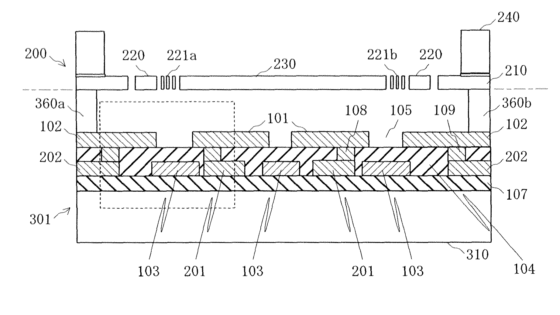
[0103]An embodiment of the present invention will now be described in detail with reference to the accompanying drawings. FIG. 1 is a sectional view of a micromirror device that is an electrostatically driven MEMS device according to the first embodiment of the present invention. Note that a mirror array is formed by one- or two-dimensionally disposing a plurality of micromirror devices shown in FIG. 1. The micromirror device according to this embodiment has a structure in which a mirror substrate 200 serving as a first substrate having a mirror and an electrode substrate 301 serving as a second substrate having electrodes are disposed in parallel.

[0104]The mirror substrate 200 has almost the same structure as that of the mirror substrate of the conventional micromirror device. The mirror substrate 200 includes a plate-shaped frame portion 210 having an opening with an almost circular shape viewed from above, a gimbal 220 having an opening with an almost circular shape viewed from a...

second embodiment

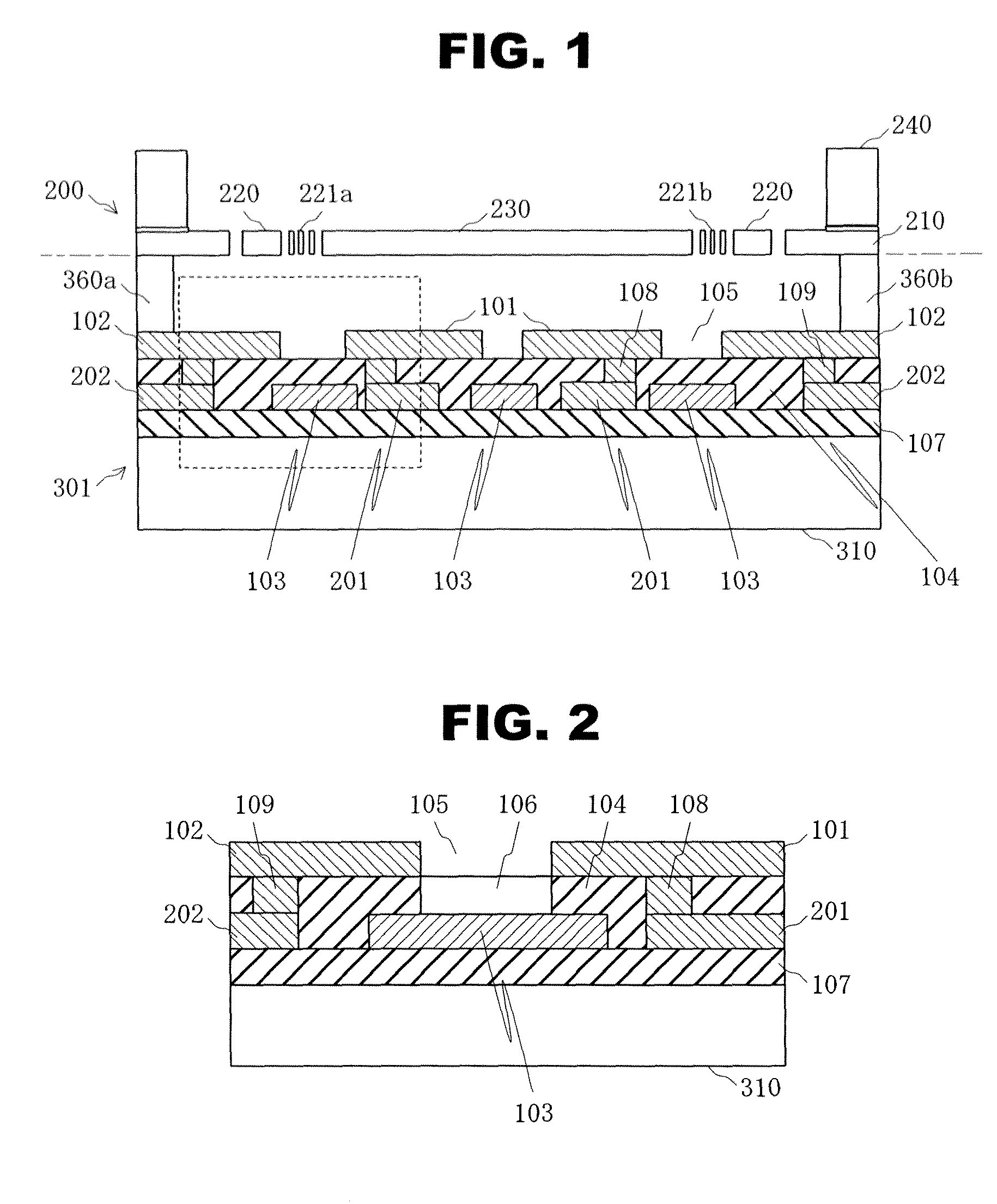
[0145]FIG. 7 is a sectional view of a micromirror device that is an electrostatically driven MEMS device according to the second embodiment of the present invention. FIG. 7 is an enlarged sectional view of a region indicated by the dotted line in FIG. 1. Note that a mirror array is formed by one- or two-dimensionally disposing a plurality of micromirror devices shown in FIG. 7.

[0146]In this embodiment, the insulating film 104 serving as a charge accumulation region exposed to the region of the gap 105 in the micromirror device according to the first embodiment is partially or wholly removed. The remaining components are the same as in the first embodiment.

[0147]In the micromirror device according to the second embodiment, an insulating film 104 under the region of a gap 105 is removed to expose a lower electrode 103 to the space. This structure can further reduce the area of the insulating film 104 exposed to the space. It is therefore possible to reduce drift of the mirror tilt ang...

third embodiment

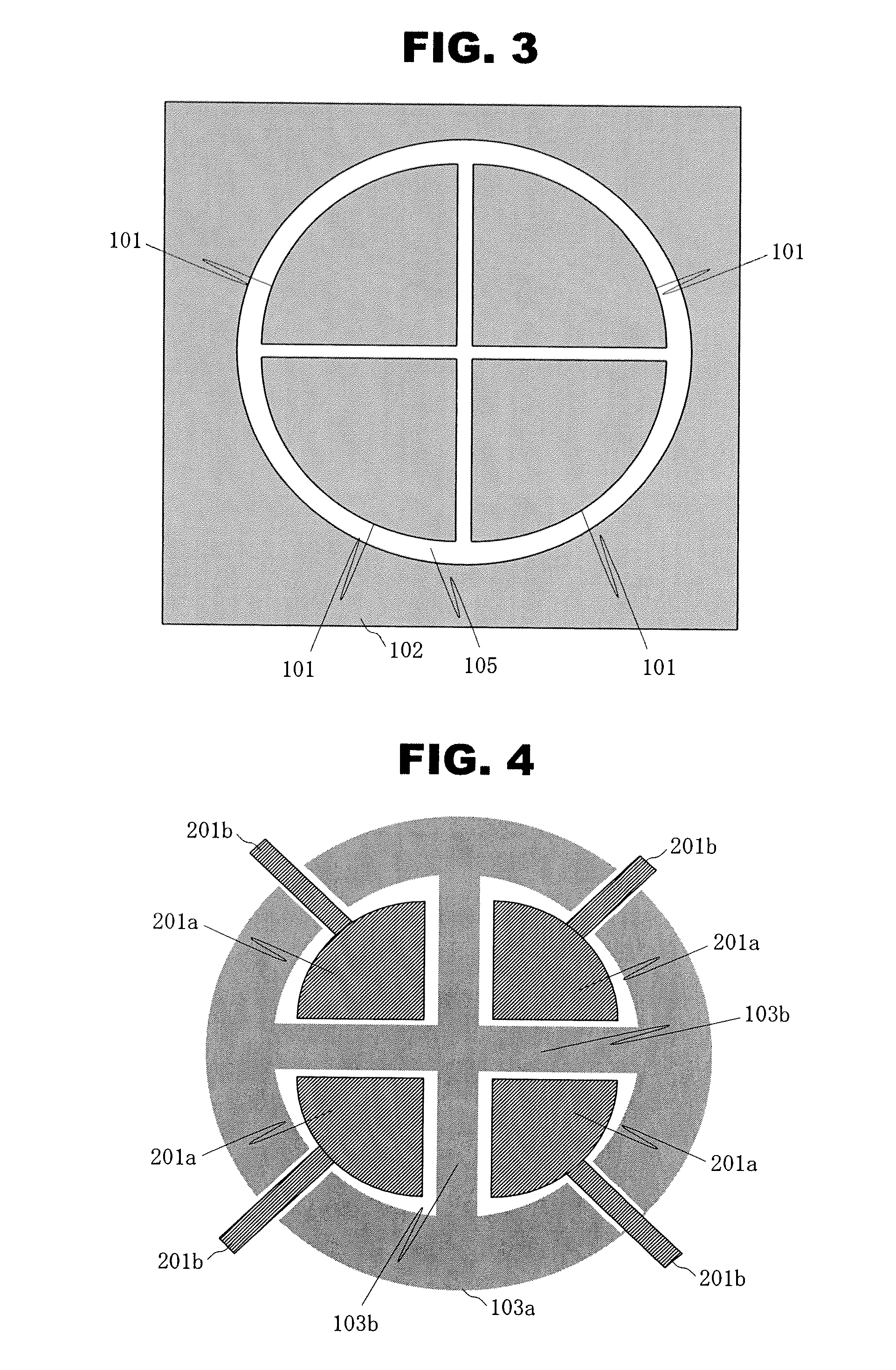
[0149]FIG. 8 is a plan view showing the electrode arrangement of a micromirror device according to the third embodiment of the present invention. This plan view illustrates underlying lower electrodes 103 and driving electrode electrical interconnections 201 seen through driving electrodes 101 and a peripheral electrode 102. A peripheral electrode electrical interconnection 202 is not illustrated in FIG. 8.

[0150]In the first embodiment, the lower electrodes 103 include the annular lower electrode 103a and the cross-shaped lower electrode 103b. In the third embodiment, a lower electrode 103a is omitted, and only a lower electrode 103a is formed. In addition, the area of driving electrode electrical interconnections 201a, which is smaller than that of the driving electrodes 101 in the first embodiment, is increased so that the driving electrode electrical interconnections 201a extend up to the region where the lower electrode 103a existed. The lower electrode 103b is formed into a cro...


PUM


Abstract

A MEMS device includes a mirror substrate (200), an electrode substrate (301) arranged so as to face the mirror substrate (200), a mirror (230) serving as a movable member rotatably supported in an opening portion of the mirror substrate (200) via support members, a driving electrode (101) arranged on an insulating film (104) on a surface of the electrode substrate (301) facing the mirror substrate (200) so as to face the mirror (230) across a gap and drive the mirror (230), and a lower electrode (103) made of a metal or a semiconductor and formed under the insulating film (104) exposed to the gap so as to be in contact with the insulating film (104).

Description

TECHNICAL FIELD[0001]The present invention relates to an electrostatically driven MEMS device used in an optical switching device for communication, a measuring device, a display, a scanner, a wavelength selective switch, or the like, and a method of manufacturing the same.BACKGROUND ART[0002]In the field of an optical network that is the basis of an Internet communication network, the optical MEMS (Micro Electro Mechanical System) technique is moving into the limelight as a technique of implementing multi-channel, WDM (Wavelength Division Multiplexing), and cost reduction, and an optical switch device to be used in optical communication has been developed using this technique. This optical switch device enables high-speed path switching without converting light into an electrical signal or without demultiplexing multiplexed light into wavelengths. As a switching device for switching an optical path, a MEMS mirror array is used (Japanese Patent Laid-Open No. 2003-57575). Such an opt...

Claims


Application Information

Patent Timeline
Patent Type & Authority Applications(United States)
IPC IPC(8): G02B26/00B05D3/10B05D5/06
CPCB81B3/0008G02B26/0841B81B2201/042B81B3/0086
Inventor UCHIYAMA, SHINGOSHIMOKAWA, FUSAOSAKATA, TOMOMISHIMOYAMA, NOBUHIROMAKIHARA, MITSUHIROUSUI, MITSUO
Owner NIPPON TELEGRAPH & TELEPHONE CORP
Why Eureka
Try Eureka