Organic electroluminescent device and organic electroluminescent apparatus

An electroluminescent device and luminescence technology, which is applied in the direction of electric solid-state devices, electrical components, semiconductor devices, etc., can solve the problems of color shift, low luminous brightness of red photon sub-pixels and green photon sub-pixels, so as to improve mobility and improve luminescence Efficiency, the effect of reducing the turn-on voltage

Pending Publication Date: 2020-07-17
YUNGU GUAN TECH CO LTD
View PDF3 Cites 0 Cited by
  • Summary
  • Abstract
  • Description
  • Claims
  • Application Information

AI Technical Summary

Problems solved by technology

In practical applications, when the blue sub-pixels are turned on, although the voltage is mainly across the blue sub-pixels, due to the better conductivity of the common hole injection layer, some of the carriers generated in the blue sub-pixels will pass through the blue sub-pixels. The common hole injection layer is migrated to the green sub-pixel and / or the red sub-pixel, and since the turn-on voltage of the red sub-pixel and the green sub-pixel is small, the red sub-pixel and / or the green sub-pixel are easy to be lit at the same time
That is, in the case of low gray scale, the luminous brightness of the red sub-pixel and / or green sub-pixel cannot strictly meet the requirements to achieve the low-brightness display effect, and the low gray scale color cast (reddish) phenomenon occurs

Method used


Image

  • Organic electroluminescent device and organic electroluminescent apparatus
  • Organic electroluminescent device and organic electroluminescent apparatus
  • Organic electroluminescent device and organic electroluminescent apparatus

Examples


Embodiment 1

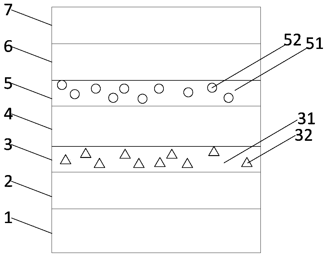
[0045] An embodiment of the present invention provides an organic electroluminescent device, such as figure 1 As shown, it includes a first electrode layer 1 , a first carrier functional layer 2 , a light emitting layer 4 and a second electrode layer 7 which are stacked. The first electrode layer 1 is an anode, and the second electrode layer 7 is a cathode, or the first electrode layer 1 is a cathode, and the second electrode layer 7 is an anode. Hereinafter, the first electrode layer 1 is used as an anode, and the second electrode layer 7 is used as a cathode as an example for illustration.

[0046] In the prior art, the process of lighting an organic electroluminescent device is to apply a certain driving voltage to the first electrode layer 1 and the second electrode layer 7, so that the carriers are transported across the potential barrier to the light-emitting layer 4, and finally emit light Layer 4 composite emits light. It can be known that the size of the potential b...

Embodiment 2

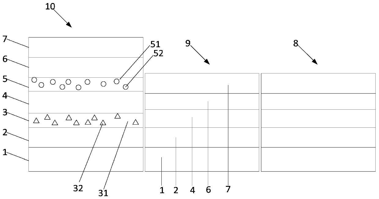
[0066] An embodiment of the present invention also provides an organic electroluminescent device, including several pixel units distributed in an array, such as image 3 As shown, each pixel unit includes a red light sub-pixel unit 8, a green light sub-pixel unit 9, and a blue light sub-pixel unit 10, and each sub-pixel unit includes a stacked first electrode layer 1, a light emitting layer 4, and a second electrode Layer 7, the light-emitting layer 4 in the red sub-pixel unit 8, the green sub-pixel unit 9 and the blue sub-pixel unit 10 is a red light-emitting layer, a green light-emitting layer and a blue light-emitting layer respectively;

[0067] The blue sub-pixel unit 10 includes the organic electroluminescence device provided in the first embodiment above. The specific content has been described in detail in Embodiment 1, and will not be repeated here.

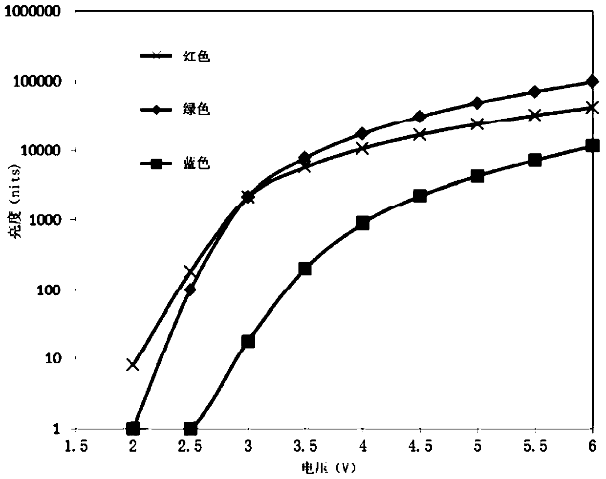
[0068]Generally, the turn-on voltage of the blue sub-pixel unit 10 is greater than the turn-on voltage of the red sub...

Embodiment 3

[0072] The embodiment of the present invention provides a specific organic electroluminescent device, including several pixel units distributed in an array, and each pixel unit includes a red sub-pixel unit 8 , a green sub-pixel unit 9 and a blue sub-pixel unit 10 .

[0073] Each sub-pixel unit includes a stacked first electrode layer 1 (anode), a first carrier functional layer 2 (electron blocking layer), a light emitting layer 4, a second carrier functional layer 6 (hole blocking layer) ) and the second electrode layer 7 (cathode), the light-emitting layer 4 in the red sub-pixel unit 8, the green sub-pixel unit 9 and the blue sub-pixel unit 10 is a red light-emitting layer, a green light-emitting layer and a blue light-emitting layer respectively.

[0074] Wherein, a P-doped layer 3 is disposed between the electron blocking layer and the blue light emitting layer in the blue light sub-pixel unit 10 . The P-doped layer 3 includes the first base material TPD and the P-dopant N...


PUM

PropertyMeasurementUnit
thicknessaaaaaaaaaa
thicknessaaaaaaaaaa

Abstract

The invention relates to the technical field of display, and discloses an organic light-emitting device and an organic electroluminescent apparatus. The organic electroluminescent device comprises a first electrode layer, a first carrier function layer, a light-emitting layer and a second electrode layer which are stacked in sequence, a P-doped layer is further arranged between the first carrier function layer and the light-emitting layer, and the P-doped layer is in direct contact with the light-emitting layer. Therefore, the energy level bending of the interface between the first carrier function layer and the light-emitting layer can be changed, the hole injection barrier at the interface between the first carrier function layer and the light-emitting layer is reduced, and the turn-on voltage of the organic electroluminescent device is effectively reduced. Specifically, when the organic electroluminescent device is applied, the turn-on voltage difference between the adjacent organicelectroluminescent devices can be reduced, so that the other organic electroluminescent devices cannot be lightened even if the generated carriers are migrated to the organic electroluminescent devices with other light-emitting colors through a common carrier functional layer, and the problem of color cast is solved.

Description

[0001] This application is a divisional application with an application date of June 29, 2018, an application number of 201810713383.5, and an invention title of "Organic Electroluminescent Device and Organic Electroluminescent Device". technical field [0002] The invention relates to the field of display technology, in particular to an organic electroluminescence device and an organic electroluminescence device. Background technique [0003] Organic electroluminescent display (English full name Organic Light Emitting Display, referred to as OLED) is an active light-emitting display device. Due to its advantages such as simple manufacturing process, low cost, high contrast, wide viewing angle, and low power consumption, it is expected to become the next generation of mainstream flat panel. Display technology is one of the most concerned technologies in flat panel display technology. [0004] figure 1 The voltage-brightness curves of the RGB three-color sub-pixels in the ex...

Claims


Application Information

Patent Timeline
Patent Type & Authority Applications(China)
IPC IPC(8): H01L51/50H01L51/52
CPCH10K50/11H10K2101/40H10K30/865H10K50/15H10K50/17H10K50/80H10K59/35H10K50/13H10K50/155H10K50/156H10K50/165H10K50/18H10K71/135
Inventor 李维维何麟李梦真田景文李田田
Owner YUNGU GUAN TECH CO LTD
Why Eureka
Try Eureka