Green light diode with interpenetration interaction structure and method of manufacturing the same

A diode and green light technology, applied in semiconductor/solid-state device manufacturing, electrical components, electric solid-state devices, etc., can solve problems such as changes in luminous intensity and luminous color, increased device manufacturing costs, and short device life

Inactive Publication Date: 2009-02-18
TAIYUAN UNIV OF TECH
View PDF0 Cites 4 Cited by
  • Summary
  • Abstract
  • Description
  • Claims
  • Application Information

AI Technical Summary

Problems solved by technology

[0002] Organic light-emitting diode OLED, because of its high luminous brightness, easy realization of large-area color flat-panel display, low-voltage DC drive, easy to match with integrated circuits, and has the advantages of full curing, wide viewing angle, rich colors, and self-illumination, is widely used in flat-panel displays and The field of lighting has a very wide application prospect. At present, red, green and blue organic electroluminescent diodes with three primary colors have been produced, but the device has a short life and low efficiency, which limits the promotion and application. To solve this problem, a On the one hand, develop luminescent materials with excellent performance, on the other hand, improve the device structure
[0003] At present, the structure of organic light-emitting diodes has many forms. In the early single-layer OLED devices, the transport capacity of the injected electrons or holes in this layer is very different, resulting in poor luminous efficiency of the device. Due to the improved carrier injection, transport and recombination, the device efficiency is effectively improved, but the device efficiency is still low. Later, a buffer layer was added to the device to reduce hole injection. Or add a hole blocking layer to limit the excess holes in the light-emitting area, but this technology requires the support of a buffer layer or barrier layer material with excellent performance, which will increase the manufacturing cost of the device and increase the turn-on voltage; Some adopt optical microcavity structure, and use the microcavity resonance effect to improve the device efficiency, but the preparation process of this structure is complicated, and the luminous intensity and luminous color change with the viewing angle
[0004] At present, the interfaces of stacked structures of organic light-emitting diodes are all flat interfaces. Generally, the transport materials used in OLEDs have better transport capabilities for holes than electrons. Therefore, in double-layer or triple-layer OLEDs, it is necessary The energy level structure is used to confine holes and electrons near the interface between the hole transport layer and the light-emitting layer, and recombine to emit light. Due to the excess holes at the interface, cationic radicals are generated in the light-emitting region, resulting in fluorescence quenching, which shortens the life of the device. short

Method used


Image

  • Green light diode with interpenetration interaction structure and method of manufacturing the same
  • Green light diode with interpenetration interaction structure and method of manufacturing the same
  • Green light diode with interpenetration interaction structure and method of manufacturing the same

Examples


Embodiment Construction

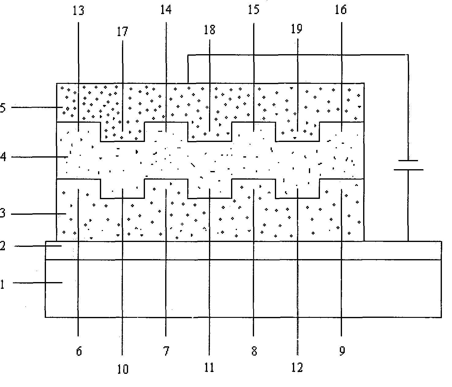
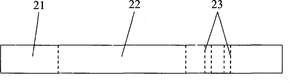
[0124] The present invention will be further described below in conjunction with accompanying drawing:

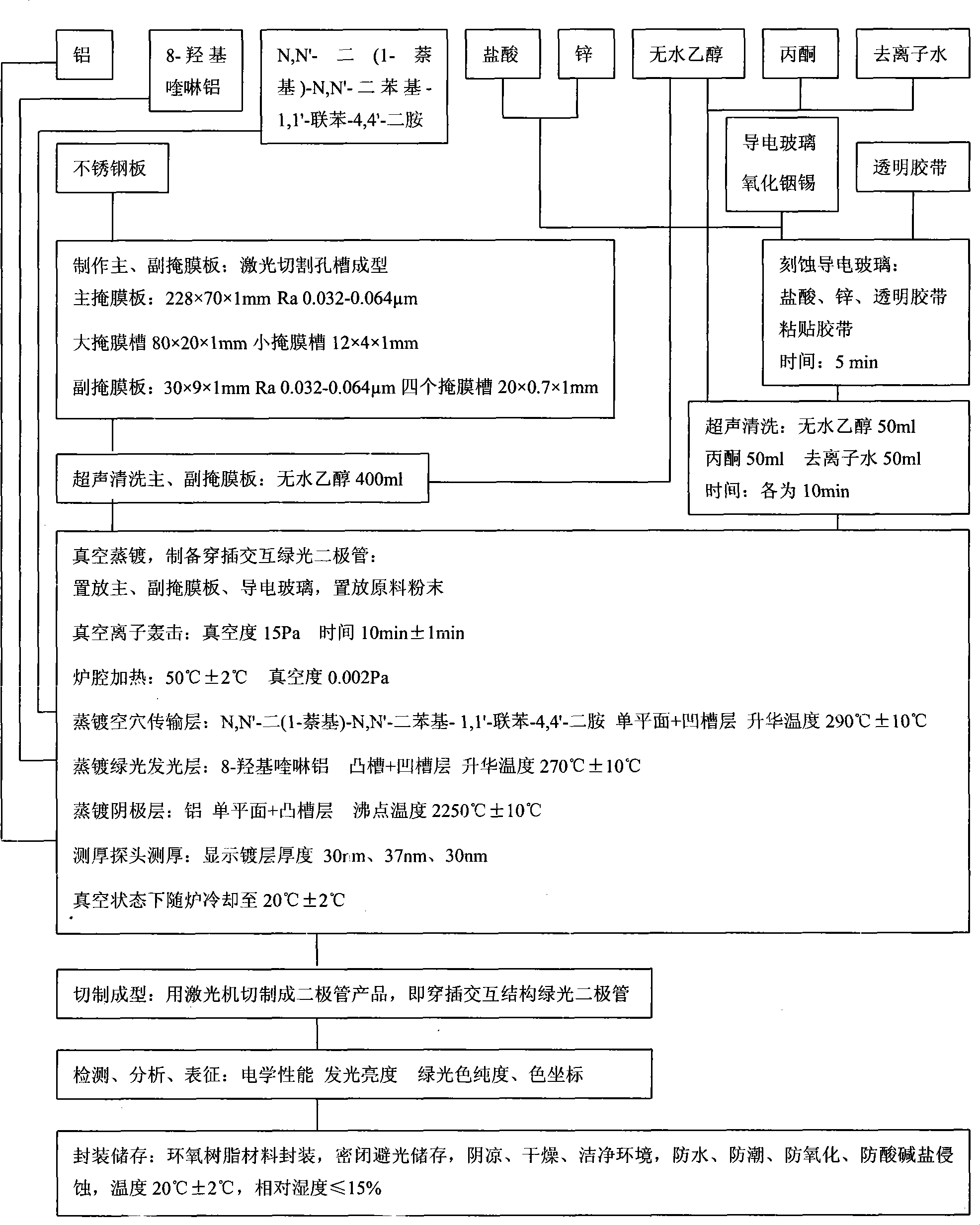
[0125] figure 1 Shown is the flow chart of the preparation process, which must be strictly carried out according to the preparation process parameters and operated step by step.

[0126] The amount of chemical substances required for preparation is determined within a preset range, with grams, milliliters, millimeters, micrometers, and nanometers as measurement units, and for industrial production, kilograms, liters, millimeters, micrometers, and nanometers The unit of measurement, the thickness of the flat layer and convex-concave layer of the green light diode is measured in nanometers.

[0127] Preparation of the desired N,N'-bis(1-naphthyl)-N,N'-diphenyl-1,1'-biphenyl-4,4'-diamine, 8-hydroxyquinoline aluminum, aluminum Strict weighing is required, and the fineness and purity are controlled, and no impurities are allowed to intervene to prevent the formation of by-pro...


PUM


Abstract

This invention is related to a green light diode with interpenetrating alternate structure and manufacturing method. The diode adopts the design of interpenetrating alternate structure. A conductive glass anode layer is a dual-plane layer. A cavity transmission layer is a single plane+ a convex groove layer. A luminous layer is a recess+ a convex groove layer. A cathode is a single plane+ a convex groove layer. Each convex groove is correspondingly matched with the recess and interpenetrated and alternated so that a structure of plane+ convex layer+ plane layer is formed. The interpenetrating alternate structure is capable of extending a current carrier complex interface and a contact interface of metal cathode layer, improving the electronic injection, reducing the generation of positive ion and increasing the complex ratio of the current carrier. A convex-concave film is film-formed by mutually displacing main and secondary mask plates. An evaporation material is converted into a film layer from a solidity-gaseity-solidity in a vacuum evaporation furnace under the condition that the vacuum degree is not greater than 0.002 Pa and the temperature is 50 degrees Celsius. This method has short technical process, and the luminous efficiency of the component can be improved about 70%; the low voltage for lightening is 2.7V; the good color purity of green light is 0.4829; the color coordinate is that X is 0.2707 and Y is 0.5267. This invention supplies a gap of scientific research of this structure, such as the light emitting diode.

Description

technical field [0001] The invention relates to a green light diode with an interspersed alternating structure and a preparation method, belonging to the technical field of design and preparation of organic electroluminescent materials and light emitting devices. Background technique [0002] Organic light-emitting diode OLED, because of its high luminous brightness, easy realization of large-area color flat-panel display, low-voltage DC drive, easy to match with integrated circuits, and has the advantages of full curing, wide viewing angle, rich colors, and self-illumination, is widely used in flat-panel displays and The field of lighting has a very wide application prospect. At present, red, green and blue organic electroluminescent diodes with three primary colors have been produced, but the device has a short life and low efficiency, which limits the promotion and application. To solve this problem, a On the one hand, it develops luminescent materials with excellent perf...

Claims


Application Information

Patent Timeline
Patent Type & Authority Applications(China)
IPC IPC(8): H01L51/56H01L51/50
Inventor 房晓红张志强樊文浩郝玉英王华许并社
Owner TAIYUAN UNIV OF TECH
Why Eureka
Try Eureka