Low-RCS ultra-wideband metamaterial wave absorber with insensitive polarization and capable of transmitting visible light
A visible light and ultra-broadband technology, applied in the direction of electrical components, antennas, etc., can solve the problems of low radar scattering cross-sectional area, low profile, etc., and achieve the effects of good angular stability, large application potential, and easy processing
- Summary
- Abstract
- Description
- Claims
- Application Information
AI Technical Summary
Problems solved by technology
Method used
Image

Examples
specific Embodiment approach 1
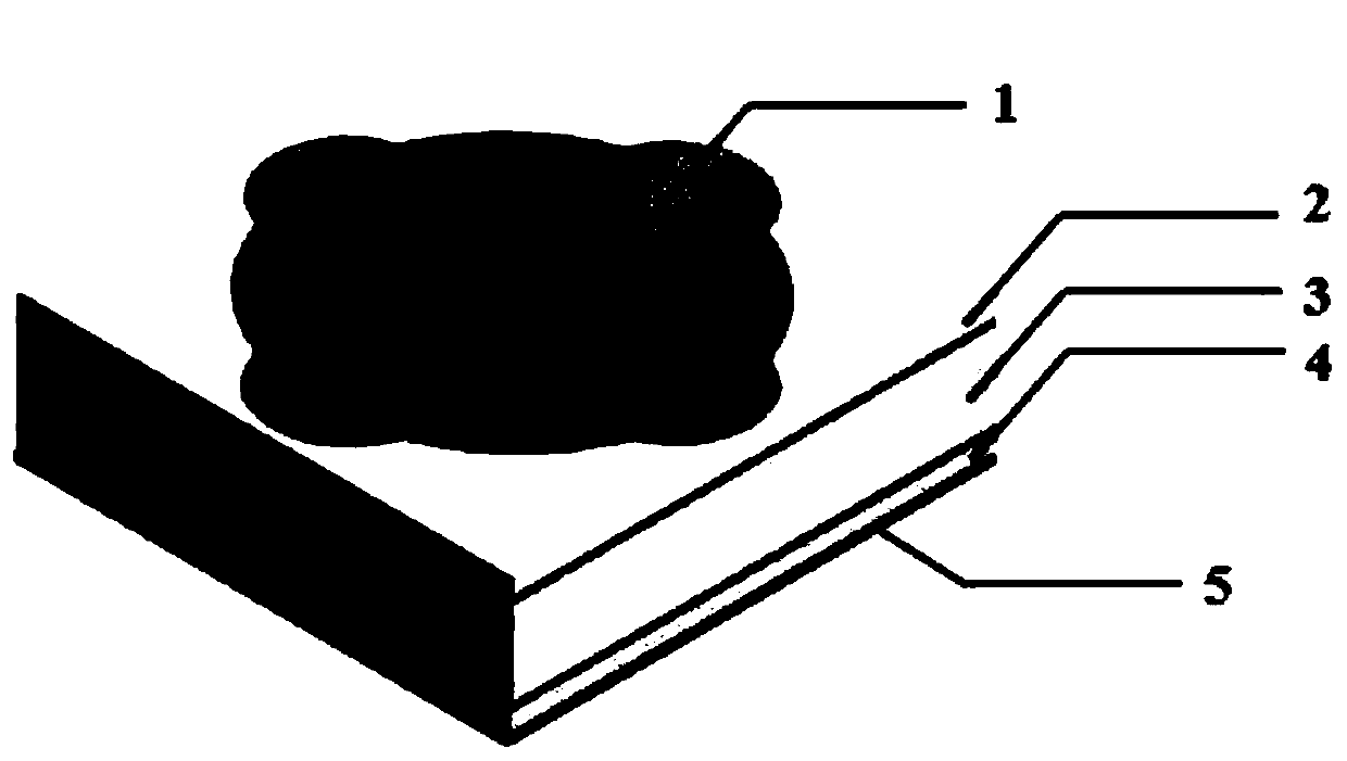
[0028] Specific implementation mode one: combine Figures 1 to 2 Specifically, this embodiment is a polarization-insensitive low-RCS ultra-broadband ultra-material absorber that transmits visible light. It consists of a patterned resistive film layer, a first transparent substrate, a middle transparent medium layer, and Composed of a second transparent substrate and a transparent conductive film;
[0029] The thickness of the patterned resistive film layer is 0.01 μm to 3 μm; the thickness of the first transparent substrate and the second transparent substrate are both 0.05mm to 2mm; the thickness of the middle transparent medium layer is 1mm to 8mm; The thickness of the transparent conductive film is 0.01 μm to 3 μm;
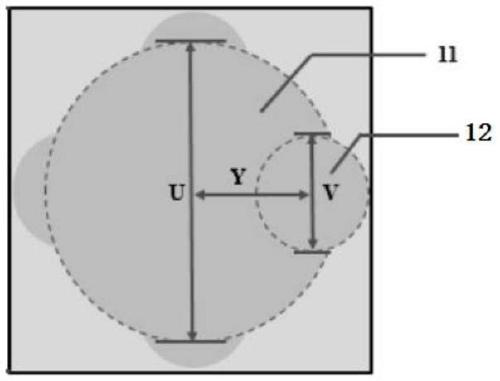
[0030] The patterned resistive film layer is composed of N×M transparent patterned resistive film units in the array; the N≥12 columns, the M≥12 rows, and the adjacent transparent patterned resistive film units The minimum distance is 0.1mm ~ 5mm;
[0031] T...
specific Embodiment approach 2
[0037] Embodiment 2: This embodiment is different from Embodiment 1 in that: the material of the intermediate transparent medium layer is one or both of transparent polymers and transparent inorganic materials. Others are the same as in the first embodiment.
specific Embodiment approach 3
[0038] Embodiment 3: This embodiment differs from Embodiment 1 or Embodiment 2 in that: the middle transparent medium layer is air, specifically, the surrounding support frame is prepared from a transparent composite material, and the first transparent substrate is used as the top , with the second transparent substrate as the bottom, and the interior is filled with air. Others are the same as in the first or second embodiment.
PUM
| Property | Measurement | Unit |
|---|---|---|
| Thickness | aaaaa | aaaaa |
| Thickness | aaaaa | aaaaa |
| Thickness | aaaaa | aaaaa |
Abstract
Description
Claims
Application Information
 - Generate Ideas
- Intellectual Property
- Life Sciences
- Materials
- Tech Scout
- Unparalleled Data Quality
- Higher Quality Content
- 60% Fewer Hallucinations
Browse by: Latest US Patents, China's latest patents, Technical Efficacy Thesaurus, Application Domain, Technology Topic, Popular Technical Reports.
© 2025 PatSnap. All rights reserved.Legal|Privacy policy|Modern Slavery Act Transparency Statement|Sitemap|About US| Contact US: help@patsnap.com