
A nano-superconducting quantum interference device and its preparation method

A superconducting quantum interference and nanotechnology, which is applied in the manufacture/processing of superconducting devices, superconducting parts, and superconducting devices, etc., can solve the problems of high preparation cost, difficulty in large-scale integration and application, poor repeatability, etc. The effect of small size, precise preparation and simple preparation process

Active Publication Date: 2022-03-25
SHANGHAI INST OF MICROSYSTEM & INFORMATION TECH CHINESE ACAD OF SCI
View PDF14 Cites 0 Cited by
  • Summary
  • Abstract
  • Description
  • Claims
  • Application Information

AI Technical Summary

Problems solved by technology

[0005] In view of the shortcomings of the prior art described above, the purpose of this application is to provide a nano-superconducting quantum interference device and its preparation method, which is used to solve the problem of poor on-chip repeatability, high manufacturing cost, It is not easy to integrate applications on a large scale

Method used


Image

  • A nano-superconducting quantum interference device and its preparation method
  • A nano-superconducting quantum interference device and its preparation method
  • A nano-superconducting quantum interference device and its preparation method

Examples


Embodiment Construction

[0041] The technical solutions in the embodiments of the present invention will be clearly and completely described below with reference to the accompanying drawings in the embodiments of the present invention. Obviously, the described embodiments are only some, but not all, embodiments of the present invention. Based on the embodiments of the present invention, all other embodiments obtained by those of ordinary skill in the art without creative work fall within the protection scope of the present invention.

[0042] Reference herein to "one embodiment" or "an embodiment" refers to a particular feature, structure, or characteristic that may be included in at least one implementation of the present invention. In the description of the present invention, it should be understood that the orientation or positional relationship indicated by the terms "upper", "lower", "top", "bottom", etc. is based on the orientation or positional relationship shown in the accompanying drawings, o...


PUM

PropertyMeasurementUnit
thicknessaaaaaaaaaa
thicknessaaaaaaaaaa
thicknessaaaaaaaaaa

Abstract

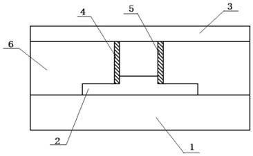
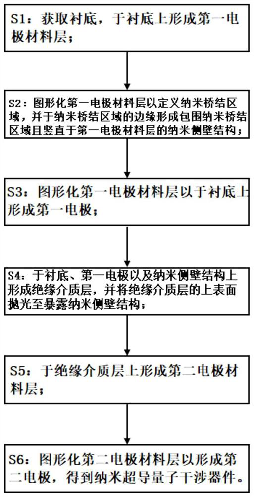
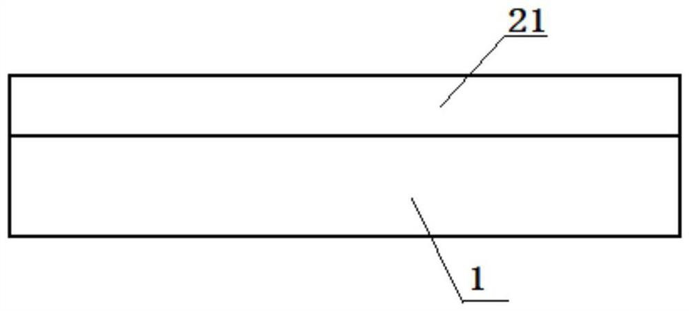
The present application provides a nano-superconducting quantum interference device and a preparation method thereof. The nano-superconducting quantum interference device includes: a first electrode formed on a substrate from bottom to top, a nano-side wall structure, and a second electrode; wherein, The nano sidewall structure includes a first sidewall and a second sidewall vertical between the first electrode and the second electrode, and the two ends of the first sidewall and the second sidewall are respectively connected The first electrode and the second electrode form two parallel nano-bridge junctions. The nano-superconducting quantum interference device of the present application uses the redeposition principle of atoms in the etching process to form a nano-side wall structure vertical to the substrate to form a superconducting ring vertical to the substrate, which has a small size and can Array, large-scale integration and other advantages.

Description

technical field [0001] The invention relates to the field of superconducting device structure design, in particular to a nanometer superconducting quantum interference device and a preparation method thereof. Background technique [0002] A superconducting quantum interference device (SQUID) is a device made of weakly connected Josephson structures in a superconducting loop. It can convert the changing magnetic flux into a voltage or current signal, that is, it can convert the weak magnetic field into The change is converted into a measurable voltage or current signal, so it can be used to detect changes in weak magnetic fields. Many superconducting active devices are prepared on the basis of SQUIDs, among which the core devices of magnetic sensors, digital logic circuits, amplifiers and other equipment are SQUIDs, which have quantum-level resistance to weak magnetic field changes unmatched by conventional sensors. Sensitive response characteristics. [0003] In recent yea...

Claims


Application Information

Patent Timeline
Patent Type & Authority Patents(China)
IPC IPC(8): H01L39/06H01L39/08H01L39/24H10N60/82H10N60/01H10N60/83
CPCH10N60/82H10N60/83H10N60/0156
Inventor 应利良许婉宁任洁王镇
Owner SHANGHAI INST OF MICROSYSTEM & INFORMATION TECH CHINESE ACAD OF SCI
Learn More