Method and apparatus for detecting key pattern

A detection method and pattern technology, applied in measurement devices, character and pattern recognition, semiconductor/solid-state device testing/measurement, etc., can solve the problem of time required for key patterns

Pending Publication Date: 2020-08-04
DISCO CORP
View PDF3 Cites 0 Cited by
  • Summary
  • Abstract
  • Description
  • Claims
  • Application Information

AI Technical Summary

Problems solved by technology

Therefore, when detecting the position of the key pattern while searching for the key pattern while forming a plurality of captured images, it is necessary to make the formation of the captured image stand by every time, so the detection of the position of the key pattern takes a lot of time.

Method used


Image

  • Method and apparatus for detecting key pattern
  • Method and apparatus for detecting key pattern
  • Method and apparatus for detecting key pattern

Examples


Embodiment Construction

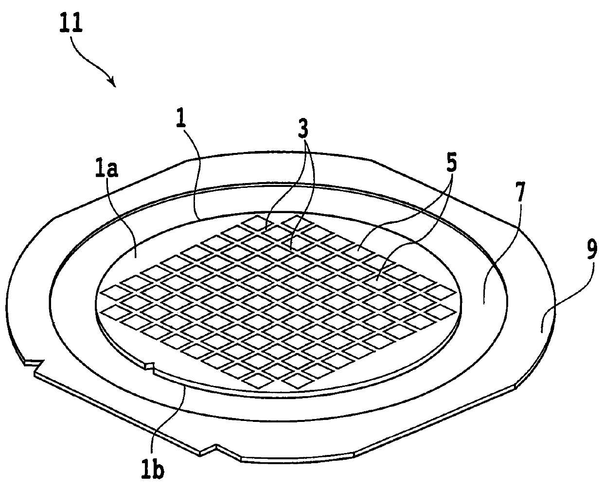
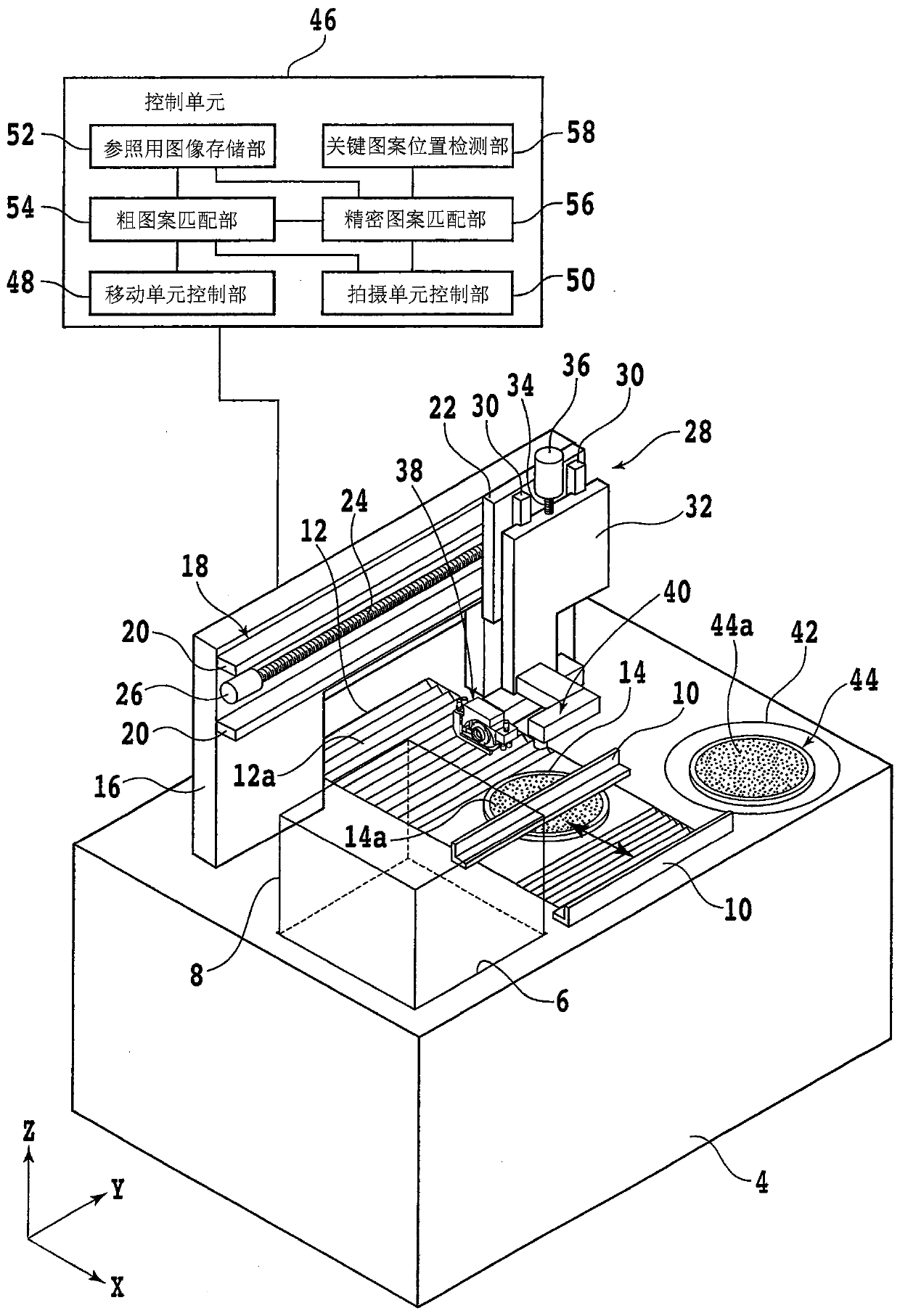
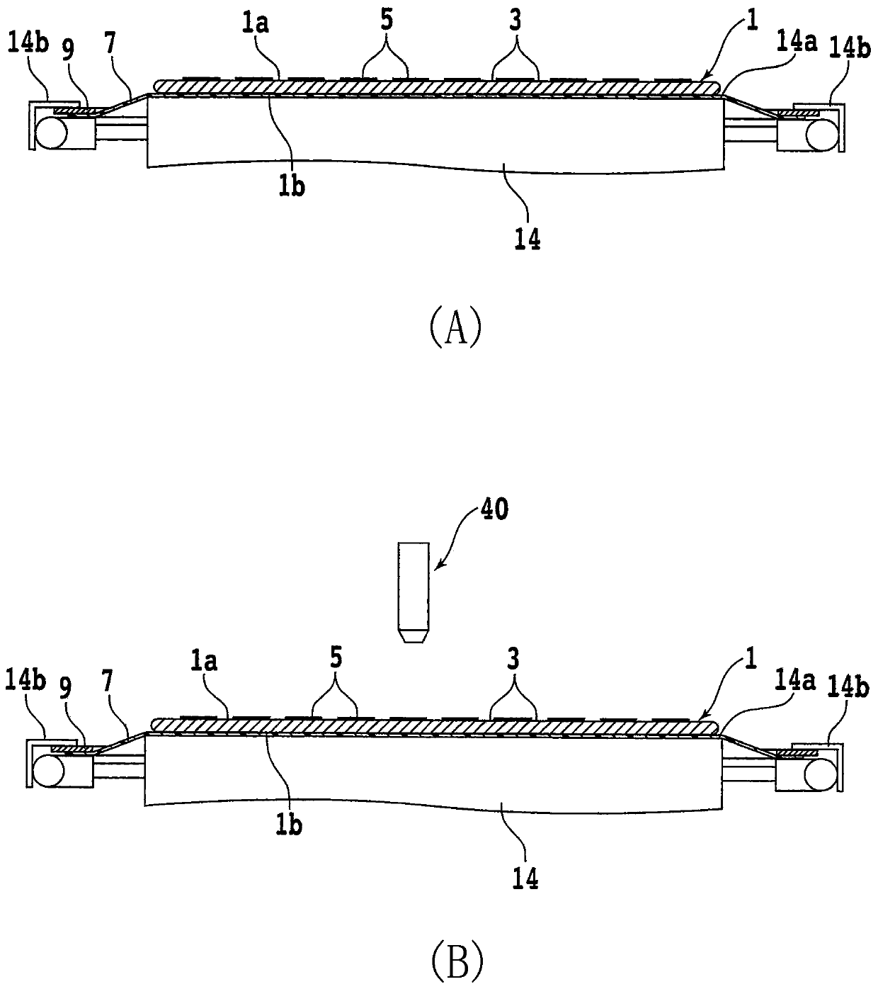
[0032] An embodiment of one embodiment of the present invention will be described with reference to the drawings. According to the method and device for detecting a key pattern of the present embodiment, it is possible to detect the position of the key pattern included in the object in a short time by taking an image of the object to be inspected. First, an object to be detected having a key pattern will be described.

[0033] The object to be detected is, for example, a substantially disk-shaped wafer made of Si (silicon), SiC (silicon carbide), GaN (gallium nitride), GaAs (gallium arsenide), or other semiconductor materials. Alternatively, the object to be detected is a substrate made of a material such as sapphire, glass, quartz, or the like. In addition, the object to be detected may be a package substrate or the like including a plurality of device chips sealed with mold resin or the like.

[0034] figure 1 It is a perspective view schematically showing a wafer 1 as an...


PUM


Abstract

A method and apparatus for detecting a key pattern, which can detect the position of the key pattern in short time, are provided. The method detects the position of the key pattern of a detected object, and comprises a rough key pattern detection step, namely a step of, while relatively moving a holding unit holding the detected object and an imaging unit, shooting the detected object by utilizingthe imaging unit to form multiple rough images, performing pattern matching on the multiple rough images and a reference image that reflects the key pattern to detect a multiple rough image reflecting the key pattern; a key pattern precision detection step, namely a step of shooting the detected object according to the relative position of the imaging unit and the holding unit when the detected multiple rough image is formed so as to form a precision photographed image, and performing pattern matching on the precision photographed image and the reference image to detect the key pattern included in the precision photographed image; and a key pattern position detection step for detecting the position of the detected key pattern.

Description

technical field [0001] The present invention relates to a method for detecting a key pattern from an object to be detected containing the key pattern and a device capable of detecting the key pattern from the object to be detected. Background technique [0002] In the manufacturing process of device chips used in electronic equipment, first, on the front surface of the semiconductor wafer, a plurality of dividing lines called streets are set to intersect each other, and devices are formed in the regions divided by the streets. . Then, when the wafer is diced along the spaced lanes, individual device chips can be formed. [0003] Dividing of the wafer is performed, for example, by a cutting device having a cutting unit. The cutting unit has a main shaft as an axis of rotation and a cutting tool attached to one end of the main shaft. The wafer is divided when the wafer is cut by rotating the spindle to rotate the cutting tool and plunging the rotating cutting tool along the...

Claims


Application Information

Patent Timeline
Patent Type & Authority Applications(China)
IPC IPC(8): H01L21/66G01N21/84
CPCH01L22/12H01L22/20G01N21/84H01L21/67294H01L21/78H01L21/67092G06F18/22
Inventor 高乘佑
Owner DISCO CORP
Why Eureka
Try Eureka