nis 2 Enhanced graphene-based SERS device and preparation method thereof
A graphene-based and graphene-based technology, applied in the field of NiS2-enhanced graphene-based SERS devices, can solve problems such as insufficient detection accuracy and strong dependence on excitation light sources, so as to broaden the application range, increase detection sensitivity, and enhance Raman signal intensity Effect
- Summary
- Abstract
- Description
- Claims
- Application Information
AI Technical Summary
Problems solved by technology
Method used
Image
Examples
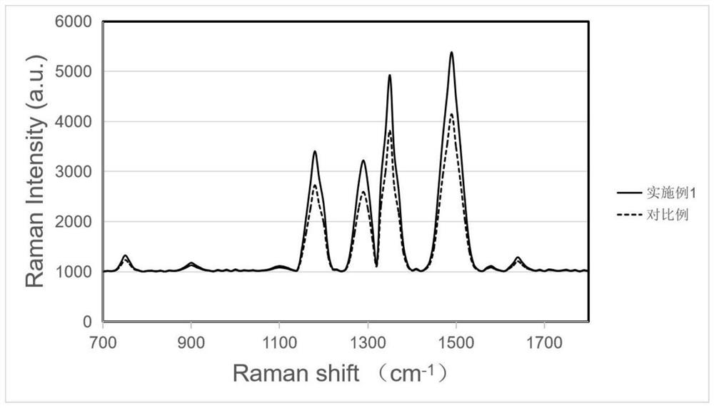
Embodiment 1
[0030] A kind of NiS 2 Enhanced graphene-based SERS device, the specific structure of which is M-NiS 2 / NiS-graphene, where M is a noble metal nanolayer, NiS 2 / NiS for alternate NiS 2 And NiS nano-multilayer structure.
[0031] Wherein, the thickness of the noble metal nano layer is 20nm, and the noble metal is Au. The number of layers of the nano-multilayer structure is 10 layers, and each layer of NiS 2 The thickness of NiS is 3nm, and the thickness of each layer of NiS is 3nm.
[0032] The NiS 2 A method for preparing an enhanced graphene-based SERS device, comprising the following steps:
[0033] (1) Using polystyrene colloidal sphere template as substrate, chemical vapor deposition of graphene layer on its surface;
[0034] (2) Atomic layer deposition of alternating NiS on the surface of the graphene layer 2 and NiS nano-multilayer structure;
[0035] (3) In alternating NiS 2 Magnetron sputtering of noble metal nanolayers on the surface of NiS nanometer multila...
Embodiment 2
[0045] A kind of NiS 2 Enhanced graphene-based SERS device, the specific structure of which is M-NiS 2 / NiS-graphene, where M is a noble metal nanolayer, NiS 2 / NiS for alternate NiS 2 And NiS nano-multilayer structure.
[0046] Wherein, the thickness of the noble metal nano layer is 5-50nm, and the noble metal is Ag. The number of layers of the nano-multilayer structure is 20 layers, and each layer of NiS 2 The thickness of NiS is 1 nm, and the thickness of each layer of NiS is 1 nm.
[0047] The NiS 2 A method for preparing an enhanced graphene-based SERS device, comprising the following steps:
[0048] (1) Using polystyrene colloidal sphere template as substrate, chemical vapor deposition of graphene layer on its surface;
[0049] (2) Atomic layer deposition of alternating NiS on the surface of the graphene layer 2 and NiS nano-multilayer structure;
[0050](3) In alternating NiS 2 Magnetron sputtering of noble metal nanolayers on the surface of NiS nanometer mult...
Embodiment 3
[0060] A kind of NiS 2 Enhanced graphene-based SERS device, the specific structure of which is M-NiS 2 / NiS-graphene, where M is a noble metal nanolayer, NiS 2 / NiS for alternate NiS 2 And NiS nano-multilayer structure.
[0061] Wherein, the thickness of the noble metal nano layer is 5-50nm, and the noble metal is Cu. The number of layers of the nano-multilayer structure is 5 layers, each layer of NiS 2 The thickness of NiS is 5 nm, and the thickness of each layer of NiS is 5 nm.
[0062] The NiS 2 A method for preparing an enhanced graphene-based SERS device, comprising the following steps:
[0063] (1) Using polystyrene colloidal sphere template as substrate, chemical vapor deposition of graphene layer on its surface;
[0064] (2) Atomic layer deposition of alternating NiS on the surface of the graphene layer 2 and NiS nano-multilayer structure;
[0065] (3) In alternating NiS 2 Magnetron sputtering of noble metal nanolayers on the surface of NiS nanometer multilay...
PUM
| Property | Measurement | Unit |
|---|---|---|
| thickness | aaaaa | aaaaa |
| thickness | aaaaa | aaaaa |
| thickness | aaaaa | aaaaa |
Abstract
Description
Claims
Application Information
