
Surface-enhanced Raman scattering active substrate and preparation method thereof
A surface-enhanced Raman and active substrate technology, applied in Raman scattering, material excitation analysis, etc., can solve the problems of easy aggregation of nanoparticles, unsatisfactory enhancement effect, unsatisfactory reuse rate, and unstable substrate performance. Effects of high detection sensitivity, high electric field strength and lifetime of photogenerated carriers, and high reuse rate
Patent Information
- Authority / Receiving Office
- CN · China
- Patent Type
- Patents(China)
- Current Assignee / Owner
- Publication Date
- 2018-05-29
Smart Images
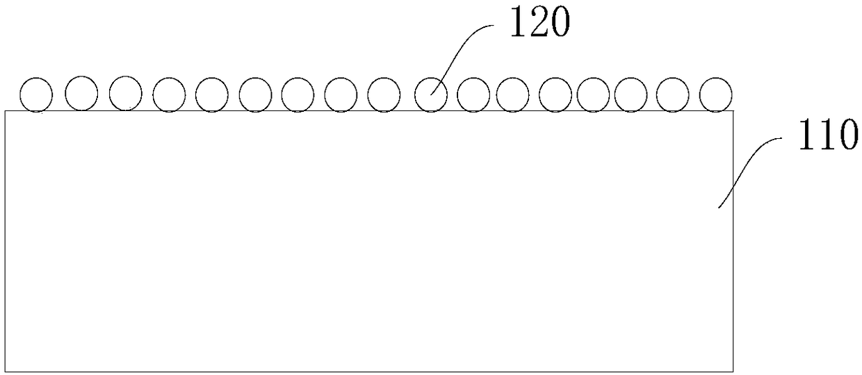
Figure 1 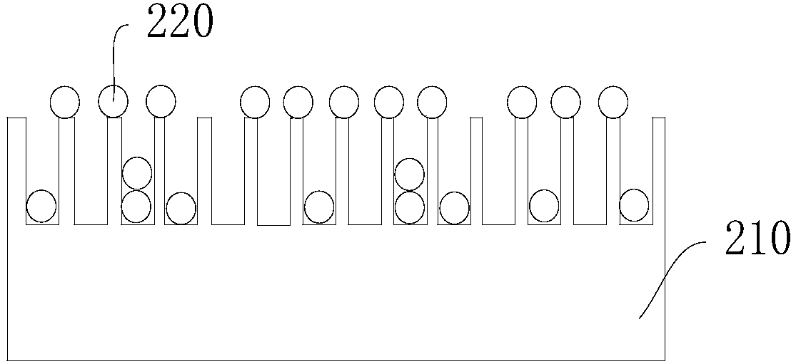
Figure 2 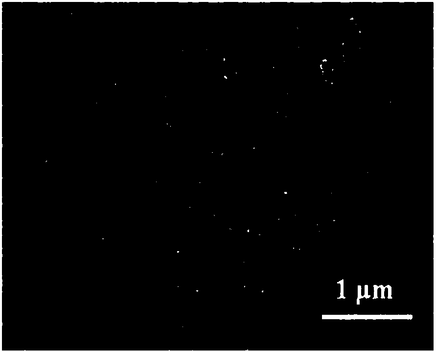
Figure 3
Abstract
Description
technical field
[0001] The invention relates to the technical fields of surface nanoscience, electrochemistry, biological science and laser Raman detection, in particular to a preparation method of a high-responsivity surface-enhanced Raman scattering active substrate. Background technique
[0002] Surface-enhanced Raman scattering (Surface-enhanced Raman scattering, SERS) spectroscopy, due to its extremely high sensitivity, can study the structural information of substances at the molecular level and realize the detection of single molecules, and has become a promising surface spectroscopy technology. . Among them, precious metals such as silver, gold, copper and alkali metals have high SERS activity, and silver has the strongest enhancement ability, followed by gold and copper; at the same time, the activity of SERS substrate is largely the same as that of metal nanomaterial The size and shape of the particles are related to the surface topography of the supporting substr...
Examples
Embodiment 1
[0025] a) Perform photoelectrochemical etching treatment on the surface of the GaN substrate: wash the GaN substrate with acetone, ethanol and deionized water in sequence, immerse the GaN substrate in 0.5M / L dilute sulfuric acid, and add a bias voltage of 3V and UV light source, anode etching for 15min. Of course, in other embodiments, etching may also be performed by immersing in an acidic solution such as hydrofluoric acid. After the etching is completed, it is cleaned with deionized water, so that the GaN substrate 110 with a porous and ravine shape is formed.
[0026] b) Using cyclic voltammetry, deposit Au nanoparticles 120 on the surface of the GaN substrate to prepare an Au-GaN-based SERS active substrate: 1 mM / L HAuCl 4 Add 1M / L NaCl (or KNO 3 or KCl) as the electrolyte, using cyclic voltammetry to deposit Au nanoparticles 120 on the surface of the GaN substrate. In a preferred embodiment, the scanning voltage range is -2.0-0.5V, the scanning rate is 50mV / s, and the...
Embodiment 2
[0029] a) The surface of the GaN substrate is subjected to photoelectrochemical etching treatment: the GaN substrate is cleaned with acetone, ethanol and deionized water in sequence, and then dried with nitrogen; the GaN substrate is immersed in 0.5M / L dilute sulfuric acid, and Add a bias voltage of 5V and an ultraviolet light source, etch the anode for 45 minutes; wash with deionized water after etching, and blow dry with nitrogen, thus forming a GaN substrate 110 with a porous groove shape.
[0030] b) Using cyclic voltammetry, deposit Au nanoparticles 120 on the surface of the GaN substrate to prepare an Au-GaN-based SERS active substrate: 1 mM / L HAuCl 4 Add 0.5M / L NaCl (or KNO 3 ) as an electrolyte, Au nanoparticles 120 are deposited on the surface of the GaN substrate by cyclic voltammetry. In a preferred embodiment, the scanning voltage range is -2.0-0.5V, the scanning rate is 50mV / s, and the number of scanning cycles is 20. After the deposition was completed, it was t...
Embodiment 3
[0033] a) Electrochemical etching treatment is performed on the surface of the GaN substrate: the GaN substrate is washed with acetone, ethanol and deionized water in sequence; the substrate is immersed in ionic liquid 1-butyl-3-methylimidazole perchlorate, And add a bias voltage of 3V, react for 40 minutes, carry out anodic etching on the GaN substrate, and rinse with deionized water after etching, thus forming a GaN substrate 110 with a porous and ravine shape, the SEM image of which is shown in FIG. 3 .
[0034] b) Using cyclic voltammetry, deposit Au nanoparticles 120 on the surface of the GaN substrate to prepare an Au-GaN-based SERS active substrate: 1 mM / L HAuCl 4 Add 0.5M / L NaCl (or KNO 3 ) as an electrolyte, Au nanoparticles 120 are deposited on the surface of the GaN substrate by cyclic voltammetry. In a preferred embodiment, the scanning voltage range is -2.0-0.5V, the scanning rate is 50mV / s, and the number of scanning cycles is 15. After the deposition was compl...