A kind of preparation method of Raman enhanced substrate
A substrate and Raman technology, applied in Raman scattering, material excitation analysis, etc., can solve the problem of poor Raman enhancement effect on copper surface, and achieve low cost effect
- Summary
- Abstract
- Description
- Claims
- Application Information
AI Technical Summary
Problems solved by technology
Method used
Image
Examples
Embodiment 1
[0029] A method for preparing a Raman enhanced substrate, comprising the following steps:
[0030] Step 1: Add 21mg of copper chloride dihydrate, 50mg of glucose and 90mg of cetylamine into 10mL of deionized water, stir and mix for 10min to obtain a precursor solution;
[0031] Step 2: Put the aluminum sheet into the precursor solution prepared in step 1, and stir for 3-10 hours until a uniform blue colloid is formed, and a small amount of free copper ions undergoes a displacement reaction with aluminum to form a seed crystal;
[0032] Step 3: Transfer the colloid prepared in step 2 to an 85°C oil bath for reaction, and the color of the colloid gradually changes from blue to brown. Because the surface energy of aluminum is smaller than that of the newly synthesized copper nanoparticles, coupled with the influence of seed crystals, The newly synthesized copper nanoparticles tend to attach to aluminum, and after 6 hours of reaction deposition, aluminum flakes with copper attache...
Embodiment 2
[0037] Compared with Example 1 in this example: the quality of hexadecylamine is 180 mg, and the remaining parameters and steps are the same as in Example 1.
[0038] figure 1 (b) is the surface morphology of the Raman-enhanced substrate obtained in Example 2, indicating that the surface of the Raman-enhanced substrate obtained in Example 2 is a rod-shaped structure, about 5 μm long and about 1 μm wide. Due to the lightning rod effect, surface plasmons will gather in the The rod-shaped tip part, and this structure with a large aspect ratio is conducive to the transmission of charges, so that the electromagnetic field strength in this area increases sharply, thereby enhancing the Raman signal.
[0039] figure 2 It is an optical image of a water droplet on the Raman-enhanced substrate obtained in Example 2; its contact angle is about 146.3°, which shows the good hydrophobicity of the substrate, which is conducive to improving the Raman signal intensity.
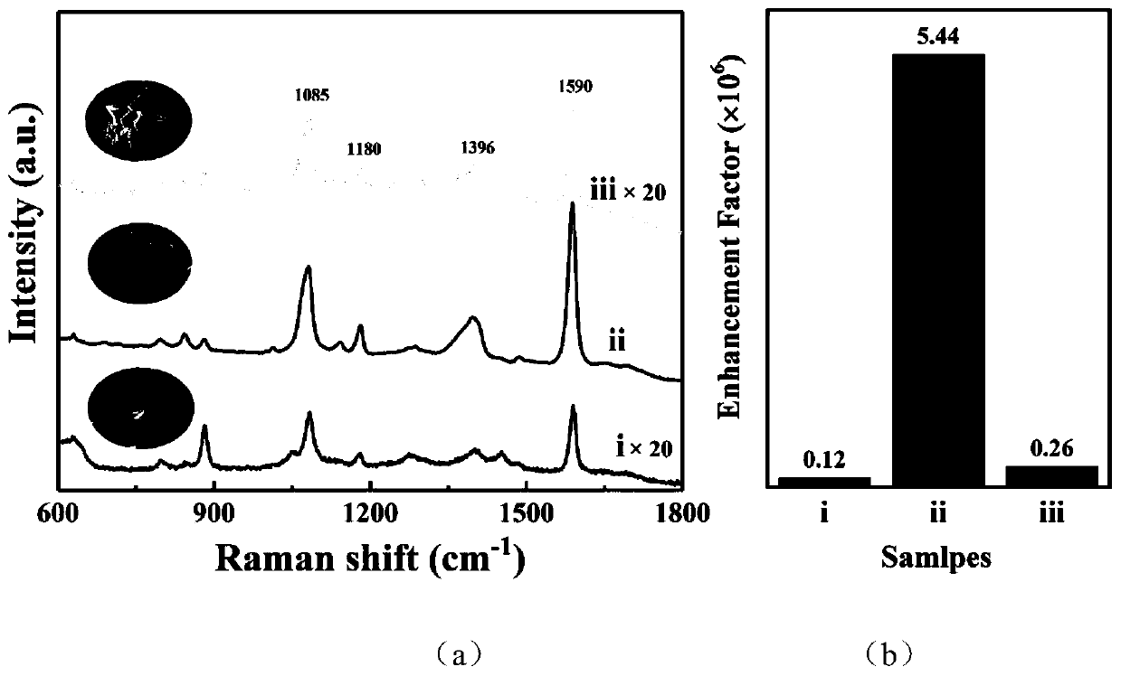
[0040] image 3 The...
Embodiment 3
[0043] Compared with Example 1 in this example: the mass of hexadecylamine is 240 mg, and the remaining parameters and steps are the same as in Example 1.
[0044] figure 1 (c) is the surface morphology of the Raman-enhanced substrate obtained in Example 3, showing that the Raman-enhanced substrate obtained in Example 3 presents clusters composed of irregular rods and petals, and the gap between these clusters can be very good The surface plasmon is confined in this region, so it has a better Raman enhancement effect.
[0045] image 3 The Raman enhancement curve of the sample iii obtained in Example 3 shows (in order to facilitate observation, the curve ordinate is enlarged 20 times), the peak position of the curve and the laser Raman spectrum of 4-mercaptobenzoic acid Figure 1 To, of which, 1590cm -1 The peak Raman intensity at is 20489counts, and the Raman enhancement factor is calculated, and the enhancement factor is 0.26×10 6 ,like image 3 (b, iii) shown.
PUM
| Property | Measurement | Unit |
|---|---|---|
| concentration | aaaaa | aaaaa |
Abstract
Description
Claims
Application Information


