Polarization doped SBD diode and preparation method thereof

A polarization doping, diode technology, applied in diodes, semiconductor/solid-state device manufacturing, electrical components, etc., can solve problems such as increasing breakdown voltage, increasing forward voltage, and reducing forward current.

Active Publication Date: 2020-08-07
SOUTH UNIVERSITY OF SCIENCE AND TECHNOLOGY OF CHINA
View PDF8 Cites 0 Cited by
  • Summary
  • Abstract
  • Description
  • Claims
  • Application Information

AI Technical Summary

Problems solved by technology

The traditional SBD structure, while increasing the height of the Schottky barrier to increase the breakdown volta

Method used


Image

  • Polarization doped SBD diode and preparation method thereof
  • Polarization doped SBD diode and preparation method thereof
  • Polarization doped SBD diode and preparation method thereof

Examples


Embodiment Construction

[0027] In order to make the object, technical solution and advantages of the present invention clearer, the present invention will be further described in detail below in conjunction with specific embodiments and with reference to the accompanying drawings.

[0028] Example This example provides a method for preparing a novel SBD diode with a terminal structure using polarized doping

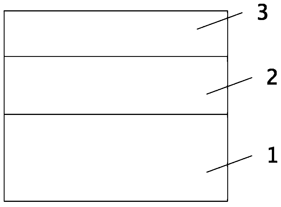
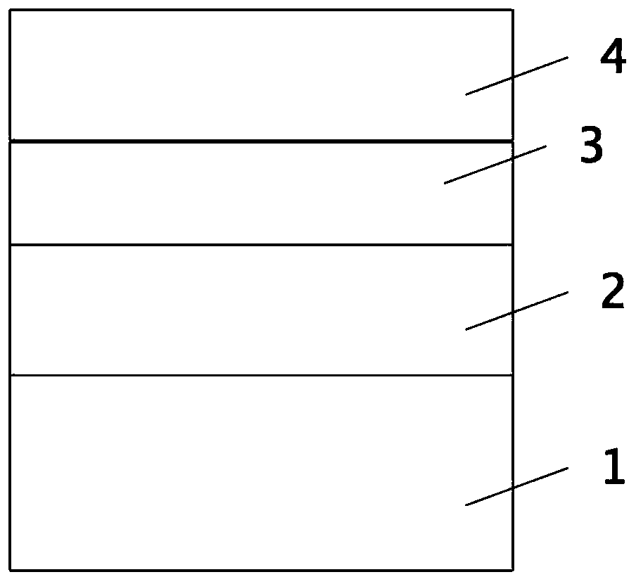
[0029] The SBD diode structure of this example is GaN substrate, n-type GaN layer, n - type GaN layer, graded doped n-type AlGaN structure, embedding the n - The high-resistance region of the GaN layer, the cathode at the bottom of the GaN substrate and the anode at the top of the GaN layer, wherein the graded doped Al x Ga 1-x The bottom layer of the N structure is an n-AlGaN layer, the top layer is an n-GaN layer, and the Al composition gradually decreases from bottom to top, where 0≤x≤1; the upper surface of the high resistance region is in common with the n-GaN layer on the top noodle.

...


PUM

PropertyMeasurementUnit
Thicknessaaaaaaaaaa
Carrier concentrationaaaaaaaaaa
Thicknessaaaaaaaaaa

Abstract

The invention provides a polarization doped SBD diode and a preparation method thereof. The SBD diode structure sequentially comprises a GaN substrate, an n type GaN layer, an n<-> type GaN layer, a gradient doped AlGaN structure, a high-resistance region embedded into the n<-> type GaN layer, a cathode located at the bottom of the GaN substrate and an anode located on the GaN layer at the top from bottom to top, wherein the bottom layer of the gradient doped AlxGa1-xN structure is an n-AlGaN layer, the top layer of the gradient doped AlxGa1-xN structure is an n-GaN layer, Al components are gradually reduced from bottom to top, x is greater than or equal to 0 and less than or equal to 1, and the upper surface of the high-resistance region and the n-GaN layer at the top are coplanar. According to the invention, polarity doping is performed on an n type region by using a gradient doping method, and the problems of low forward conduction voltage and small forward conduction current are solved while the SBD breakdown voltage is improved by using an oxide layer terminal structure.

Description

technical field [0001] The invention belongs to the field of semiconductor devices, in particular to a polarized doped SBD diode and a preparation method thereof. Background technique [0002] Schottky diode Schottky (Schottky) diode is a low-power, ultra-high-speed semiconductor device. The most notable feature is that the reverse recovery time is extremely short (can be as small as a few nanoseconds), and the forward voltage drop is only about 0.4V. It is mostly used as high-frequency, low-voltage, high-current rectifier diodes, freewheeling diodes, and protection diodes. It is also useful as rectifier diodes and small-signal detector diodes in microwave communication circuits. It is more common in communication power supplies, frequency converters, etc. In the traditional SBD structure, while increasing the height of the Schottky barrier to increase the breakdown voltage, it also has the disadvantages of increasing the forward conduction voltage and reducing the forward...

Claims


Application Information

Patent Timeline
IPC IPC(8): H01L29/06H01L29/872H01L21/329
CPCH01L29/872H01L29/66212H01L29/0684H01L29/0611
Inventor 高博刘新科
Owner SOUTH UNIVERSITY OF SCIENCE AND TECHNOLOGY OF CHINA
Why Eureka
Try Eureka