
Magnetic bias weak light triggered high-power photoconductive switch

A photoconductive switch, high-power technology, applied in electronic switches, electrical components, pulse technology, etc., can solve the problems of high cost, large volume and weight, and limited working life, so as to prevent long-term ablation, reduce current density, and improve The effect of working life

Active Publication Date: 2020-08-07
INST OF FLUID PHYSICS CHINA ACAD OF ENG PHYSICS
View PDF13 Cites 0 Cited by
  • Summary
  • Abstract
  • Description
  • Claims
  • Application Information

AI Technical Summary

Problems solved by technology

However, the general high-power photoconductive switch needs a laser with high output light energy as the trigger light source, so the volume and weight are relatively large and the cost is high. Although the photoconductive switch working in the nonlinear mode can use a laser with a small volume and weight and low cost The high-power laser diode is used as the trigger light source, but the wire current discharge formed during the conduction process leads to a rather limited working life under high-power working conditions.

Method used


Image

  • Magnetic bias weak light triggered high-power photoconductive switch
  • Magnetic bias weak light triggered high-power photoconductive switch
  • Magnetic bias weak light triggered high-power photoconductive switch

Examples


Embodiment 1

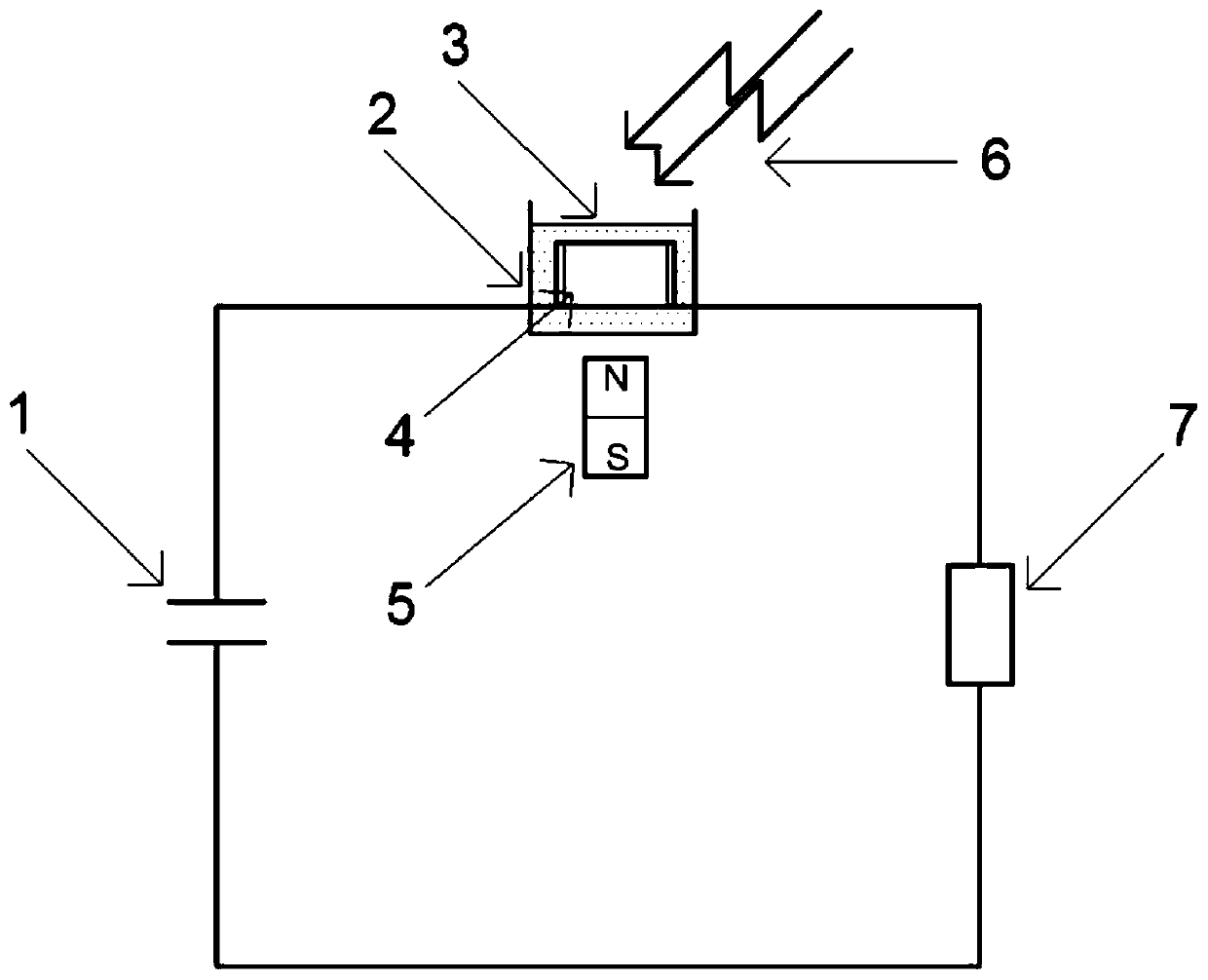
[0029] Such as figure 1 As shown, a magnetically biased weak light triggers a high-power photoconductive switch, including an insulating container 2, an insulating medium 3, a photoconductive switch 4, a magnetic field generating element 5, and a trigger light source 6, and the photoconductive switch 4 is immersed in the insulating medium 3 , the photoconductive switch 4 and the insulating medium 3 are placed together in the insulating container 2, the magnetic field generating element 5 is located under the insulating container, the magnetic field generated by the magnetic field generating element 5 is perpendicular to the direction of the electric field borne by the photoconductive switch 4, and the trigger light source 6 passes through the insulating medium 3 is irradiated onto the upper surface of the photoconductive switch 4 .

[0030] In the above technical solution, when the trigger light source 6 irradiates the photoconductive switch 4, photocarriers are generated, and...

Embodiment 2

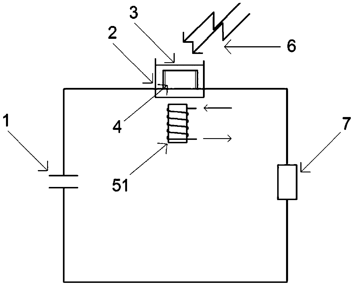
[0036] This embodiment provides an implementation similar to Embodiment 1, the difference is that the magnetic field generating element 5 uses an electromagnet 51, such as figure 2 As shown, it includes an insulating container 2, an insulating medium 3, a photoconductive switch 4, an electromagnet 51 and a trigger light source 6. The photoconductive switch 4 is immersed in the insulating medium 3, and the photoconductive switch 4 and the insulating medium 3 are placed together in the insulating container 2. Among them, the electromagnet 51 is located under the insulating container, the magnetic field generated by the electromagnet 51 is perpendicular to the direction of the electric field received by the photoconductive switch 4 , and the trigger light source 6 shines on the upper surface of the photoconductive switch 4 through the insulating medium 3 .

[0037] Preferably, the electromagnet 51 is a solenoid electromagnet, and the magnitude and direction of the bias magnetic f...

Embodiment 3

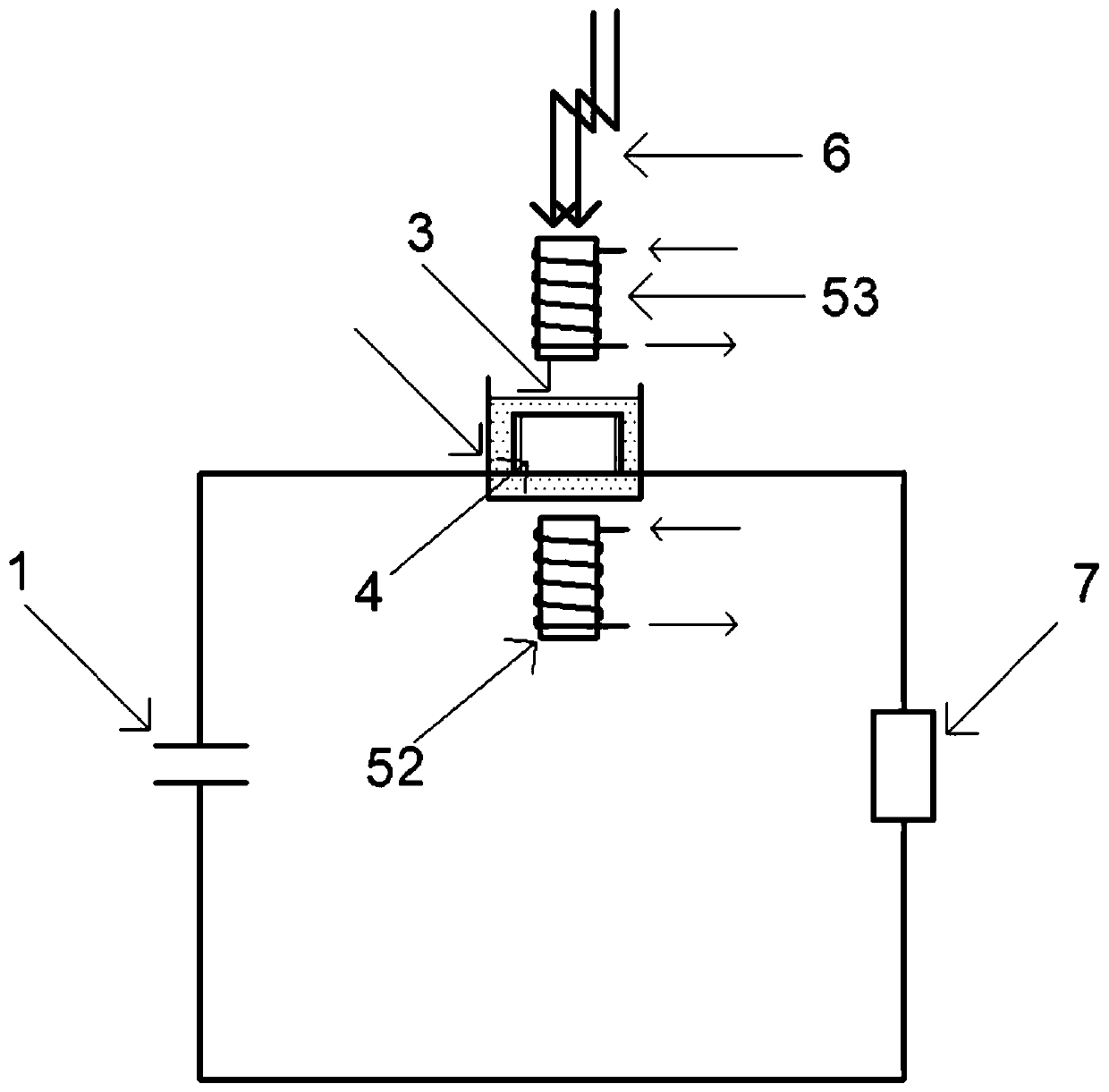
[0040] Such as image 3 As shown, in this embodiment, it includes an insulating container 2, an insulating medium 3, a photoconductive switch 4, a lower magnetic field generating element 52, an upper magnetic field generating element 53, and a trigger light source 6. The photoconductive switch 4 is immersed in the insulating medium 3, The photoconductive switch 4 and the insulating medium 3 are placed together in the insulating container 2, the lower magnetic field generating element 52 is located below the insulating container, the upper magnetic field generating element 53 is located above the insulating container, the upper magnetic field generating element 53 is a hollow structure, and the lower magnetic field generating element 52 The direction of the magnetic field generated by the upper magnetic field generating element 53 is in the same direction and the direction of the electric field received by the photoconductive switch 4 is vertical. The trigger light source 6 pass...


PUM

PropertyMeasurementUnit
diameteraaaaaaaaaa
thicknessaaaaaaaaaa

Abstract

The invention relates to the technical field of pulse power. The invention discloses a magnetic bias weak light triggered high-power photoconductive switch, which comprises a photoconductive switch, an insulating medium, an insulating container, a magnetic field generating element and a trigger laser, wherein the photoconductive switch is immersed in the insulating medium; the insulating medium isused for increasing the surface withstand voltage strength of the photoconductive switch; the photoconductive switch and the insulating medium are both arranged in the insulating container; the magnetic field generating element is arranged on the outer side of the insulating container; a magnetic field generated by the magnetic field generating element is perpendicular to an internal electric field of the photoconductive switch; and the trigger laser is used for controlling conduction of the photoconductive switch. Laser triggering is adopted, photoelectric isolation is realized between trigger control and high voltage; in addition, magnetic field bias is adopted to enable the electron multiplication direction in the photoconductive switch to deflect, so that the transverse sectional areaof carrier avalanche is increased, a current wire moves transversely, the current density of the current wire is reduced in an turning-on state, and the purpose of prolonging the service life of theweak light triggered high-power photoconductive switch is achieved.

Description

technical field [0001] The invention relates to the technical field of pulse power, in particular to a magnetically biased weak light triggering high-power photoconductive switch. Background technique [0002] The photoconductive switch is one of the key components of the pulsed power device, and its performance has an important influence on the performance of the pulsed power device. High-power photoconductive switches have the advantages of short closing time, small time jitter, high repetition frequency, photoelectric isolation, and large power capacity per unit volume, and have broad application prospects in the field of pulse power. However, the general high-power photoconductive switch needs a laser with high output light energy as the trigger light source, so the volume and weight are relatively large and the cost is high. Although the photoconductive switch working in the nonlinear mode can use a laser with a small volume and weight and low cost A high-power laser d...

Claims


Application Information

Patent Timeline
Patent Type & Authority Applications(China)
IPC IPC(8): H03K17/78
CPCH03K17/78
Inventor 付佳斌谢卫平何泱栾崇彪刘宏伟袁建强
Owner INST OF FLUID PHYSICS CHINA ACAD OF ENG PHYSICS
Learn More