
Preparation method of three-dimensional ferroelectric random access memory and three-dimensional ferroelectric random access memory

A random access memory and ferroelectric capacitor technology, which is applied in the direction of electric solid-state devices, circuits, electrical components, etc., can solve the problems of high operating voltage and low integration density of ferroelectric random access memory, and achieve low operating voltage, wide application value, and integrated high density effect

Pending Publication Date: 2020-08-11
XIANGTAN UNIV
View PDF5 Cites 1 Cited by
  • Summary
  • Abstract
  • Description
  • Claims
  • Application Information

AI Technical Summary

Problems solved by technology

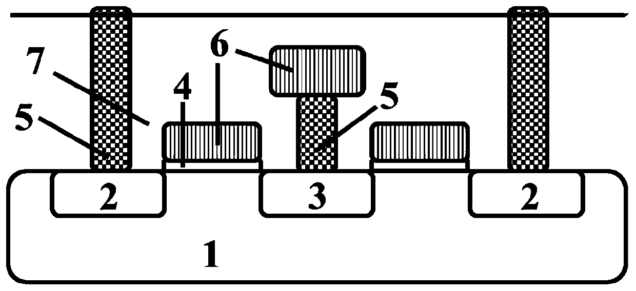
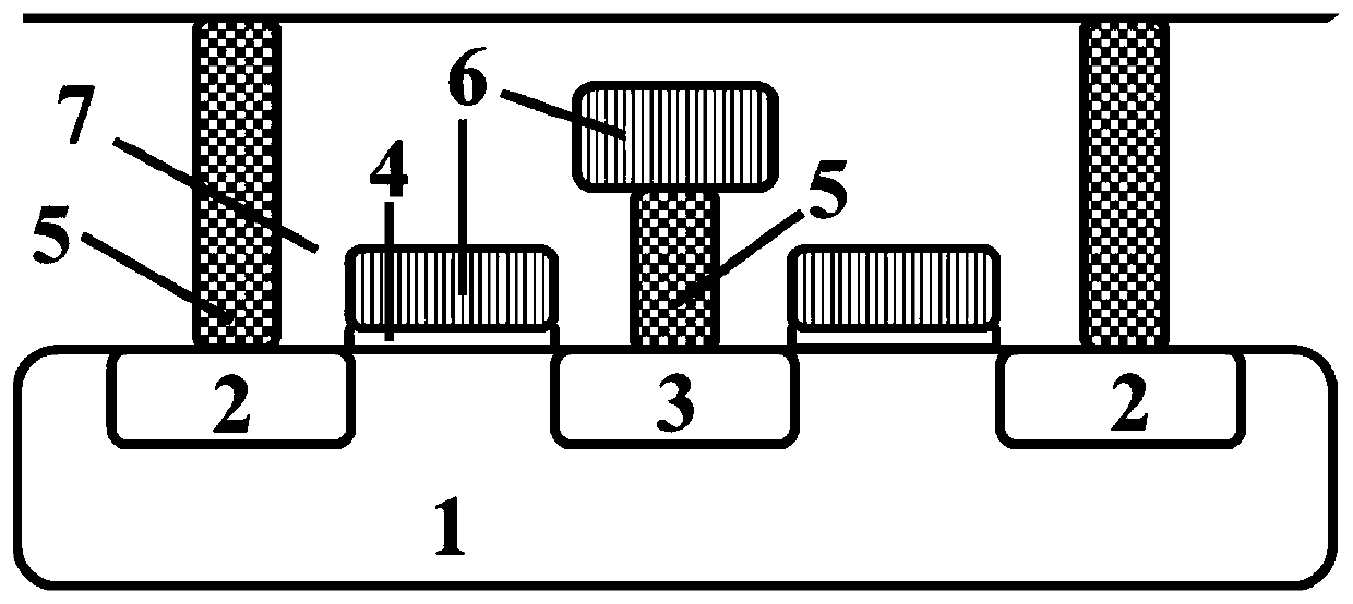
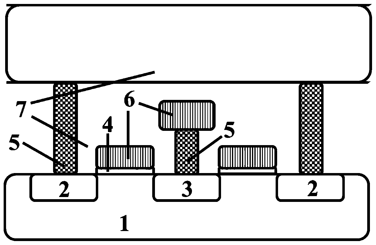
[0006] The purpose of the present invention is to provide a preparation method of a three-dimensional ferroelectric random access memory and a three-dimensional ferroelectric random access memory, so as to obtain a high-density three-dimensional ferroelectric random access memory, so as to solve the problems of low integration density and high operating voltage of the existing ferroelectric random access memory

Method used


Image

  • Preparation method of three-dimensional ferroelectric random access memory and three-dimensional ferroelectric random access memory
  • Preparation method of three-dimensional ferroelectric random access memory and three-dimensional ferroelectric random access memory
  • Preparation method of three-dimensional ferroelectric random access memory and three-dimensional ferroelectric random access memory

Examples


Embodiment Construction

[0040] In order to make the object, technical solution and advantages of the present invention clearer, the present invention will be further described in detail below in combination with specific embodiments and with reference to the accompanying drawings. It should be understood that these descriptions are exemplary only, and are not intended to limit the scope of the present invention. Also, in the following description, descriptions of well-known structures and techniques are omitted to avoid unnecessarily obscuring the concept of the present invention.

[0041] The present invention will be described in detail below in conjunction with the accompanying drawings and embodiments.

[0042] The preparation method of the three-dimensional ferroelectric random access memory provided by the present invention comprises the following steps:

[0043] S1: Transistors are prepared based on a CMOS process, and the transistors are fabricated on a traditional CMOS process line.

[004...


PUM


Abstract

The invention provides a preparation method of a three-dimensional ferroelectric random access memory and the three-dimensional ferroelectric random access memory. The preparation method comprises thefollowing steps: while preparing a transistor based on a CMOS process, vertically integrating each ferroelectric storage unit of a three-dimensional ferroelectric capacitor on the transistor in sequence to obtain the three-dimensional ferroelectric random access memory. The ferroelectric storage unit of the three-dimensional ferroelectric capacitor sequentially comprises an interlayer medium (7),a capacitor bottom electrode (9), a ferroelectric film (10) and a capacitor top electrode (11) which are vertically deposited. A ferroelectric capacitor is integrated into a complementary metal oxidesemiconductor (CMOS), and a capacitor structure is converted from a plane to a three-dimensional structure to increase a capacitor area, so that higher storage density is realized, and the size of astorage unit is further reduced on the premise of not reducing storage charges.

Description

technical field [0001] The invention relates to the technical field of semiconductors, in particular to a preparation method of a three-dimensional ferroelectric random access memory and a three-dimensional ferroelectric random access memory. Background technique [0002] With the continuous breakthrough and development requirements of modern information technology, the size of semiconductor storage units is continuously reduced and the integration level is also continuously improved. Therefore, higher requirements are put forward for the process technology of semiconductor storage units. The manufacturing cost of the unit is constantly increasing. In order to solve the difficulties encountered in the planar capacitor structure and pursue lower manufacturing costs, a ferroelectric random access memory with a three-dimensional capacitor structure is proposed. [0003] The storage unit of the three-dimensional ferroelectric random access memory is a MOS tube and a capacitor s...

Claims


Application Information

Patent Timeline
IPC IPC(8): H01L27/11514H01L27/11507H01L27/11509
CPCH10B53/20H10B53/40H10B53/30
Inventor 廖敏郇延伟戴思维刘兆通曾斌建周益春
Owner XIANGTAN UNIV
Learn More