Damage analysis method for heavy ion radiation silicon carbide diode under bias electric field

A silicon carbide diode, heavy ion radiation technology, applied in chemical process analysis/design, computational theoretical chemistry, instrumentation, etc., can solve problems such as device failure, microscopic damage to device materials, and impact on device electrical properties, saving time and money. Effect

Active Publication Date: 2020-08-18
XIANGTAN UNIV
View PDF6 Cites 0 Cited by
  • Summary
  • Abstract
  • Description
  • Claims
  • Application Information

AI Technical Summary

Problems solved by technology

[0005] Although the flux of heavy ions in the space environment is low, it has a strong energy loss characteristic. The incident of heavy ions on silicon carbide diodes will cause microscopic damage de

Method used


Image

  • Damage analysis method for heavy ion radiation silicon carbide diode under bias electric field
  • Damage analysis method for heavy ion radiation silicon carbide diode under bias electric field
  • Damage analysis method for heavy ion radiation silicon carbide diode under bias electric field

Examples


Embodiment

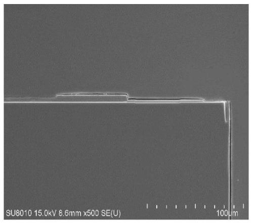
[0043] Step S1: Use FIB to cut the silicon carbide diode longitudinally, calibrate the composition of each layer of silicon carbide diode after cutting, and obtain the basic structure and material composition of the silicon carbide diode.

[0044]Among them, the longitudinal section is cut from the surface of the positive electrode of the silicon carbide diode downward, so that a relatively complete structure distribution of the diode can be obtained.

[0045] figure 1 is a cross-sectional view of a SiC JBS diode, please check figure 1 , the upper part of the figure represents the silicon carbide positive electrode metal, the middle part is the silicon carbide substrate and epitaxial layer, and the lower part is the silicon carbide negative electrode metal. It can be seen from the cross-sectional view that there is no doping concentration in the silicon carbide diode, so the epitaxial layer and the substrate are not distinguished.

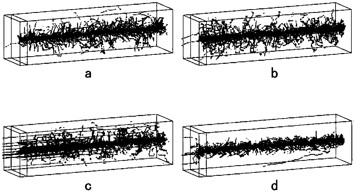
[0046] Specifically, a TEM (Transmission E...


PUM


Abstract

A damage analysis method for a heavy ion radiation silicon carbide diode under a bias electric field comprises the steps of: constructing a simulation model of a silicon carbide diode through Geant4 based on the basic structure and material composition of the silicon carbide diode, and setting the size of the bias electric field and the type and energy of incident particles in the Geant4; performing analogue simulation in Geant4: injecting incident particles into the silicon carbide diode, and simulating the particle motion trails of the incident particles in the silicon carbide diode and theinitial defect damage distribution of the silicon carbide diode under different bias electric fields; and based on the simulation model and the initial defect damage distribution, simulating a defectdamage evolution process of the silicon carbide diode through TCAD software so as to analyze the influence of defect damage on the electrical property of the silicon carbide diode. The interaction relationship between the bias electric field and the radiation damage is disclosed, and a technical basis is provided for radiation effect mechanism analysis and reliability evaluation of silicon carbidedevices.

Description

technical field [0001] The invention relates to the technical field of anti-radiation analysis of semiconductor devices, in particular to a damage analysis method for silicon carbide diodes irradiated by heavy ions under a bias electric field. Background technique [0002] In order to establish a high-efficiency, high-reliability power system, people have been working on improving power switching devices, and silicon-based diodes are the main materials for power switching devices. However, the heat dissipation performance of silicon-based diodes is poor, and it will be subject to many restrictions in high-power applications. In addition to the continuous research on silicon-based devices for many years, the performance of silicon materials is close to the limit of its intrinsic characteristics. [0003] Silicon carbide is a wide bandgap semiconductor material, its bandgap width is about three times that of silicon material, and silicon carbide material has high thermal condu...

Claims


Application Information

Patent Timeline
IPC IPC(8): G16C10/00G16C20/10G16C60/00
CPCG16C10/00G16C20/10G16C60/00
Inventor 郭红霞张鸿潘霄宇周益春张凤祁张晋新琚安安钟向丽廖敏
Owner XIANGTAN UNIV
Why Eureka
Try Eureka