Display substrate, preparation method thereof and display device

A technology for display substrates and substrates, applied in semiconductor devices, electrical components, photovoltaic power generation, etc., can solve problems such as packaging failure of display devices, and achieve the effect of low cost, easy realization, and simple process

Active Publication Date: 2020-08-18
BOE TECH GRP CO LTD
View PDF4 Cites 4 Cited by
  • Summary
  • Abstract
  • Description
  • Claims
  • Application Information

AI Technical Summary

Problems solved by technology

[0005] The technical problem to be solved by the embodiments of the present invention is to provide a display substrate and its preparation method, and a display device, so as to solve problems such as packaging failure of the display device.

Method used


Image

  • Display substrate, preparation method thereof and display device
  • Display substrate, preparation method thereof and display device
  • Display substrate, preparation method thereof and display device

Examples


Embodiment Construction

[0034] The specific implementation manners of the present invention will be further described in detail below in conjunction with the accompanying drawings and examples. The following examples are used to illustrate the present invention, but are not intended to limit the scope of the present invention. It should be noted that, in the case of no conflict, the embodiments in the present application and the features in the embodiments can be combined arbitrarily with each other.

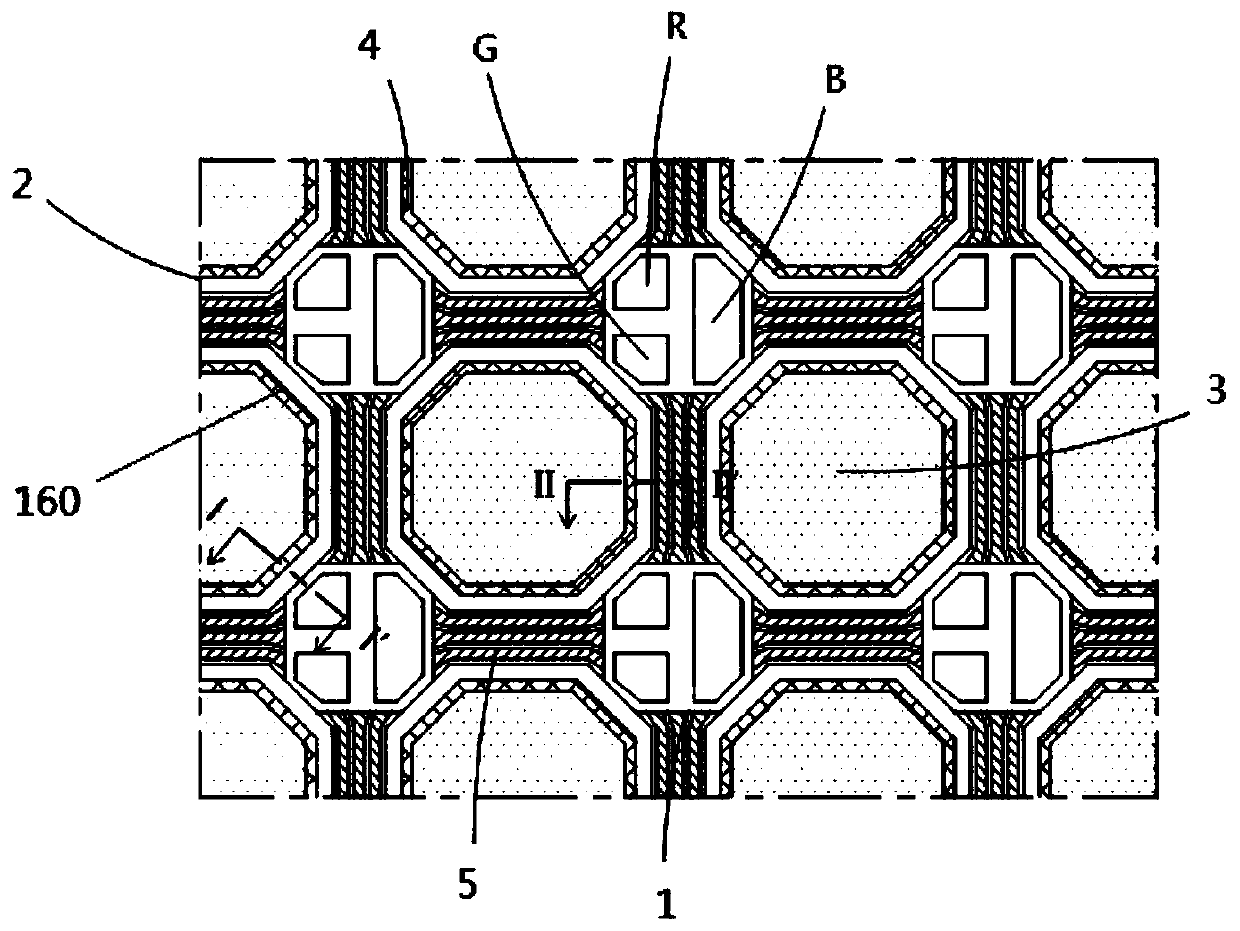
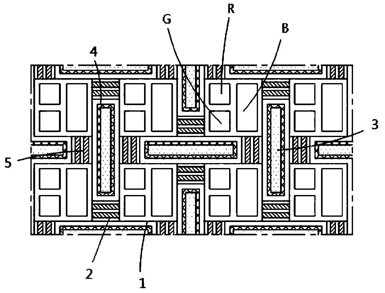
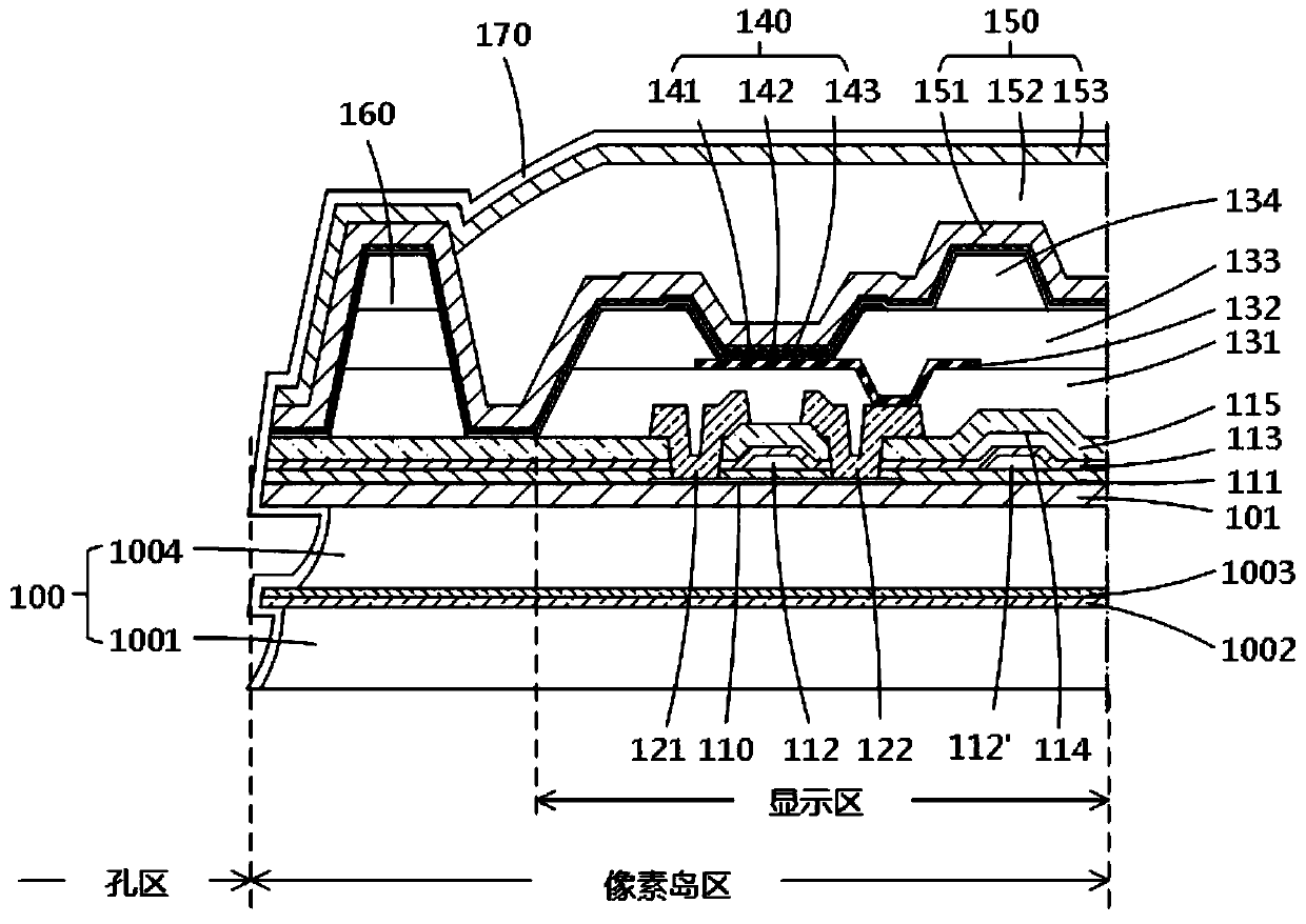
[0035] The inventors of the present application found that a flexible OLED display device with a microporous structure needs to form an encapsulation layer on the pixel island area and the connection bridge area. The encapsulation layer includes an inorganic layer and an organic layer that are superimposed. The organic layer is printed by inkjet. (IJP) post-curing process. In the preparation process of the organic layer, the organic material ink before curing is deposited on the pixel island area and t...


PUM


Abstract

The invention provides a display substrate, a preparation method thereof and a display device. The display substrate comprises a substrate, wherein the substrate is provided with a plurality of pixelisland areas which are separated from one another, hole areas arranged between adjacent pixel island areas, and connecting bridge areas for connecting the adjacent pixel island areas; a first box dam,a groove and a packaging layer covering the groove are formed on the connecting bridge area; the first box dam is located on the side, which is close to the hole area, of the connecting bridge area;the groove is formed in the side, which is away from the hole area, of the first box dam on the connecting bridge area; and the first box dam is used for preventing a packaging layer material before curing from entering the hole area, and the groove is used for guiding the packaging layer material before curing to flow in the extending direction of the first box dam so as to prevent the packaginglayer material before curing from overflowing out of the first box dam, so that the problems of packaging failure and the like of the display device are solved.

Description

technical field [0001] The invention relates to the field of display technology, in particular to a display substrate, a preparation method thereof, and a display device. Background technique [0002] Organic Light Emitting Diode (OLED) is an active light-emitting display device, which has the advantages of self-illumination, wide viewing angle, high contrast, low power consumption, wide color gamut, light and thin, and can be shaped. With the continuous development of display technology, OLED technology is increasingly used in flexible displays and transparent displays. Transparent display is an important branch of display technology. It refers to image display in a transparent state. The viewer can not only see the image in the display device, but also see the scene behind the display device, which can realize virtual reality / augmented reality ( VirtualReality / AugmentedReality, VR / AR) and 3D display functions. [0003] Currently, flexible OLED display devices usually ado...

Claims


Application Information

Patent Timeline
IPC IPC(8): H01L27/32
CPCH10K59/122H10K59/123H10K59/124H10K59/1213H10K59/1315Y02E10/549
Inventor 张子予曹方旭
Owner BOE TECH GRP CO LTD
Why Eureka
Try Eureka