Developer composition used in fields of flat panel display and semiconductors

A flat-panel display and semiconductor technology, applied in the field of surfactants, can solve the problems of residual development, slow development speed, excessive foam, etc., and achieve the effects of moderate development speed, increased concentration, and low cost

Active Publication Date: 2020-08-21
福建省佑达环保材料有限公司
View PDF7 Cites 0 Cited by
  • Summary
  • Abstract
  • Description
  • Claims
  • Application Information

AI Technical Summary

Problems solved by technology

The addition of additives brings many uncertain factors, such as excessive foam, reduced development speed, development residue, etc.

Method used


Image

  • Developer composition used in fields of flat panel display and semiconductors
  • Developer composition used in fields of flat panel display and semiconductors
  • Developer composition used in fields of flat panel display and semiconductors

Examples


experiment example

[0044] Experimental example: Determination experiment of developing performance of developing solution

[0045] In order to evaluate the developing performance of the CF developer compositions in Examples 1-12 and Comparative Examples 1-6 above, the developing performance test of the developer was carried out by the following test.

[0046] 1. Manufacturing test pieces

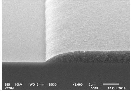
[0047] In order to evaluate the development performance of the developer composition to the photoresist, the test piece used is to spin coat a layer of 1.5 μm BM negative photoresist or R, G, B photoresist on a glass substrate of 5 cm * 5 cm, The specific treatment is as follows: After the glass substrate is thoroughly cleaned with a special cleaning agent, rinsed with ultrapure water, and blown dry with nitrogen. The photoresist was spin-coated with a spin coater at a speed of 300rpm. After vacuuming to remove most of the solvent, it was cured by heating on a flat plate at 100°C. The curing time was 150s. Th...


PUM

PropertyMeasurementUnit
thicknessaaaaaaaaaa

Abstract

The invention belongs to the technical field of surfactants, and particularly relates to a chemical preparation used in the fields of panel display and semiconductors, and the preparation is used fordeveloping a developing photoresist in the fields of panel display and semiconductors. The preparation is prepared from 10%-30% of specific Gemini type polyether nonionic surfactants with different EOvalues, 5%-20% of alkaline substances and 50%-80% of high-purity water. According to the invention, two different EO values of the specific Gemini type nonionic surfactant are mixed; the use amount of a surfactant in the developing solution can be remarkably reduced, the concentration of a stock solution of the developing solution is remarkably improved, the developing performance is effectivelyimproved, the developing solution is moderate in developing speed, clear in pattern, complete in edge, free of photoresist residues, stable in dispersion of developing residues, small in foam and lowin cost, and meanwhile, the transportation burden and cost of the high-concentration developing solution are greatly reduced.

Description

technical field [0001] The invention belongs to the technical field of surfactants, in particular to a developer composition used in the fields of flat panel displays and semiconductors, and is used for developing negative photoresists in flat panel displays and semiconductors. [0002] technical background [0003] The production process in the field of flat panel display and semiconductor involves multiple processes, some of which involve the developer of negative photoresist. The photolithography process for making devices in the flat panel display and semiconductor fields usually includes glue coating, pre-baking, exposure, development and post-baking, etc. to obtain corresponding devices. The photoresist solvent is removed during the pre-baking process, and different areas are selected for exposure through the mask plate. The exposed area can be removed by alkaline developer, and the unexposed area is left to obtain the corresponding pattern. Common developing methods i...

Claims


Application Information

Patent Timeline
Patent Type & Authority Applications(China)
IPC IPC(8): G03F7/32
CPCG03F7/322
Inventor 刘小勇侯琳熙颜如彩
Owner 福建省佑达环保材料有限公司
Why Eureka
Try Eureka