Unlock instant, AI-driven research and patent intelligence for your innovation.

Dynamic random access memory and manufacturing method thereof

A dynamic random access and memory technology, which is applied in semiconductor/solid-state device manufacturing, electric solid-state devices, semiconductor devices, etc., can solve the problems of increased resistance and affecting performance, and achieve the effect of reducing bit line resistance and improving performance

Inactive Publication Date: 2020-08-25
FUJIAN JINHUA INTEGRATED CIRCUIT CO LTD
View PDF8 Cites 2 Cited by
  • Summary
  • Abstract
  • Description
  • Claims
  • Application Information

AI Technical Summary

Problems solved by technology

However, the shrinking of the size will increase the resistance of the circuit of the memory and affect the performance

Method used


Image

  • Dynamic random access memory and manufacturing method thereof
  • Dynamic random access memory and manufacturing method thereof
  • Dynamic random access memory and manufacturing method thereof

Examples


Embodiment Construction

[0052] The following detailed description and description, with reference to the content shown in the relevant drawings, are used together to illustrate embodiments that can be implemented according to the present invention. These embodiments provide sufficient details to enable those skilled in the art to fully understand and practice the present invention. The following embodiments can be modified in structure, logic and electricity without departing from the spirit of the present disclosure, for example, the features in several different embodiments are replaced, reorganized, mixed and applied to other embodiments .

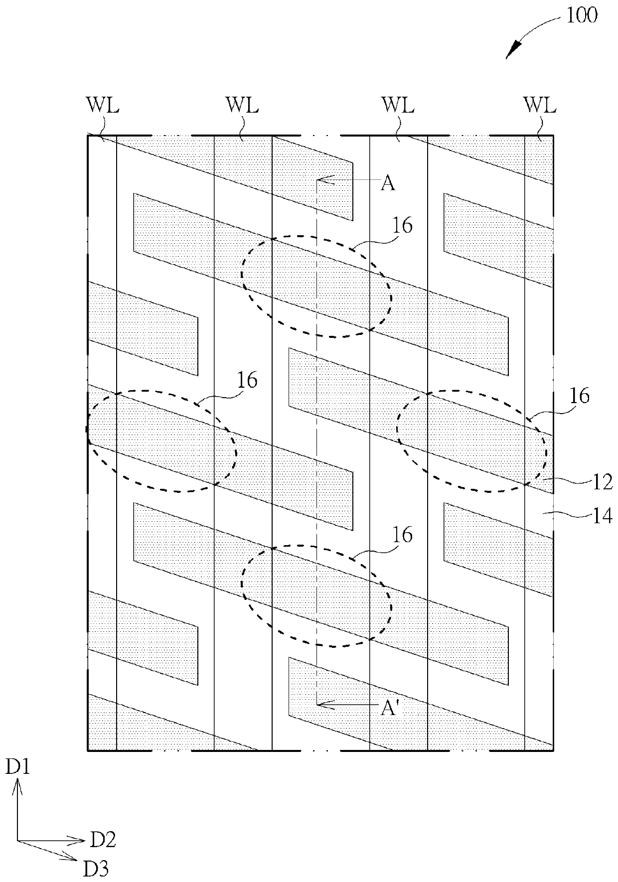
[0053] Figure 1A , Figure 1B , Figure 2A , Figure 2B , image 3 , Figure 4A and Figure 4B It is a schematic diagram of the manufacturing method steps of the DRAM 100 according to an embodiment of the present invention. Figure 1A and Figure 2A is a top view of the dynamic random access memory 100 on a plane defined by the first direction D1 and t...


PUM


Abstract

The invention discloses a method for manufacturing a dynamic random access memory, the method comprises the following steps of providing a substrate which comprises a plurality of active regions and an isolation structure surrounding the plurality of active regions; forming a bit line stacking layer on the substrate, wherein the bit line stacking layer comprises a silicon layer; patterning the bitline stack layer to form a plurality of bit lines, and forming a metal silicide on sidewalls of the silicon layer of the bit lines. According to the dynamic random access memory and the manufacturingmethod thereof provided by the invention, the metal silicide is formed on the side walls of the bit lines, so that the resistance of the bit lines can be reduced, and the efficiency is improved.

Description

technical field [0001] The invention relates to a memory and its manufacturing method, in particular to a dynamic random access memory and its manufacturing method. Background technique [0002] Dynamic random access memory (dynamic random access memory, DRAM) is a kind of volatile memory, including an array area (array area) composed of a plurality of memory cells (memory cells) and a peripheral area (peripheral area) composed of control circuits ). Each memory cell includes a transistor electrically connected to a capacitor, and the transistor controls the storage or release of charges in the capacitor to achieve the purpose of storing data. The control circuit can be positioned to each memory cell to control its data access through the word line (word line, WL) and the bit line (bit line, BL) that straddle the array area and are electrically connected to each memory cell. [0003] With the evolution of generations, the size of memory cells is gradually reduced to obtain...

Claims


Application Information

Patent Timeline
Patent Type & Authority Applications(China)
IPC IPC(8): H01L21/8242H01L27/108H10B12/00
CPCH10B12/30H10B12/482
Inventor 冯立伟
Owner FUJIAN JINHUA INTEGRATED CIRCUIT CO LTD