A semiconductor surface insulating film processing device

A technology for processing device and insulating film, applied in spraying device and other directions, can solve problems such as affecting appearance quality, wasting materials, affecting efficacy, etc., and achieves the effect of improving appearance quality and beauty, improving spraying efficiency, and avoiding waste.

Active Publication Date: 2021-08-10
江苏黎彬新材料科技有限公司
View PDF9 Cites 0 Cited by
  • Summary
  • Abstract
  • Description
  • Claims
  • Application Information

AI Technical Summary

Problems solved by technology

[0003] And produce resistive thin film with existing technology, after spraying insulating varnish sometimes thickness is too thick and can affect its effect, also can waste material, the surface after spraying insulating varnish is not processed and can be relatively rough, affects appearance quality, and existing The technology can only be sprayed on one side, after drying and forming a film, and then spraying on the other side will affect the production efficiency

Method used


Image

  • A semiconductor surface insulating film processing device
  • A semiconductor surface insulating film processing device
  • A semiconductor surface insulating film processing device

Examples


Embodiment 1

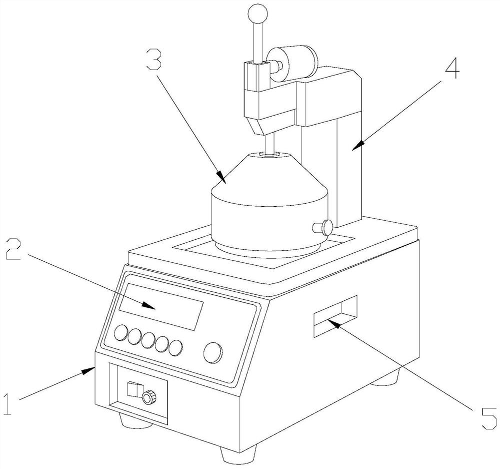
[0029] see Figure 1-Figure 3 , the present invention provides a semiconductor surface insulating film processing device, its structure includes a film spraying processing machine 1, an operation panel 2, a spraying sealing device 3, a spraying machine head 4, and a lifting groove 5, and the front end surface of the film spraying processing machine 1 is An operation panel 2 is installed on the top of the film spraying processing machine 1. A spraying machine head 4 is arranged on the top of the film spraying processing machine 1. The film spraying processing machine 1 is connected with the spraying machine head 4. The left and right sides of the film spraying processing machine 1 Lifting grooves 5 are provided on the sides, and a spraying sealing device 3 is provided at the middle position of the top of the film spraying processing machine 1, and the film spraying processing machine 1 and the spraying sealing device 3 are movably connected;

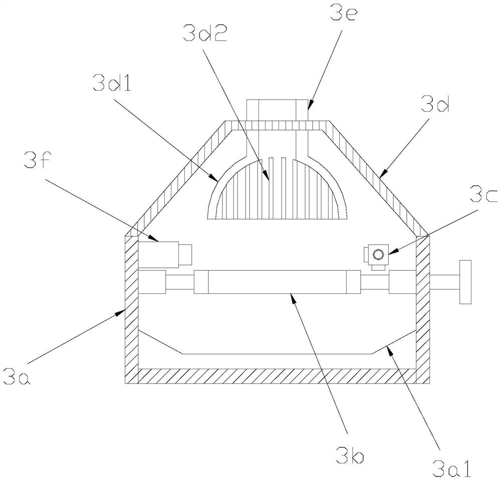
[0030] The spray sealing device 3 ...

Embodiment 2

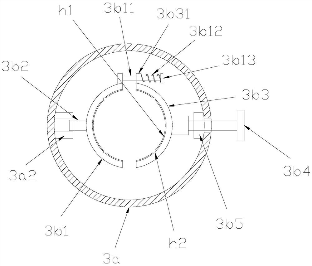
[0038] see Figure 1-Figure 5 , the present invention provides a semiconductor surface insulating film processing device, the scraping mechanism 3c is composed of a bracket 3c1, a telescopic rod 3c2, a sliding column 3c3, a storage groove 3c4, and a soft scraping strip 3c5, and the bracket 3c1 is about Both ends are provided with storage grooves 3c4 on the inner sides, and said storage grooves 3c4 are provided with telescopic rods 3c2. The column 3c3, the telescopic rod 3c2 and the sliding column 3c3 are fixedly connected, the bottom of the bracket 3c1 is provided with a soft scraping strip 3c5, and the bracket 3c1 is glued to the soft scraping strip 3c5.

[0039] The front end of the bracket 3c1 is provided with an armature 3c11, the bracket 3c1 is fixedly connected with the armature 3c11, and the rear end of the bracket 3c1 is equipped with a tension spring 3c12.

[0040] A spraying guide cover 3d1 is provided under the inner bottom end of the dustproof cover body 3d, the d...


PUM

PropertyMeasurementUnit
thicknessaaaaaaaaaa

Abstract

The invention discloses a semiconductor surface insulating film processing device, the structure of which comprises a film spraying processing machine, an operation panel, a spraying sealing device, a spraying machine head, and a lifting tank. The spraying sealing device can limit the position of a semiconductor chip through a semiconductor clamping structure Clamping, avoiding its deviation during spraying, using the included angle groove to clamp the semiconductor chip with a square structure, which improves the efficiency of clamping and spraying of semiconductor chips of different shapes, without the need for mechanical power clamping, To avoid damage to the semiconductor chip due to mechanical power failure, the spraying head can continuously spray the surface of the semiconductor chip through the rotation of the semiconductor clamping structure, and the spray sealing device scrapes off the redundant spray coating on the surface of the semiconductor chip through the scraping mechanism. Avoid waste of materials, so that the surface of the semiconductor chip will not be rough, and improve the quality and appearance of its appearance.

Description

technical field [0001] The invention relates to the technical field of semiconductor processing, in particular to a semiconductor surface insulating film processing device. Background technique [0002] At present, to insulate the surface of conductive parts without affecting the original conductive function, it mainly relies on the spraying method to cover the surface with a layer of high-resistance electrical insulation coating, and the thickness of the coating ranges from 0.00127 to 0.0127 mm. The base material of the insulating paint is mainly synthetic resins such as acetal resin, neoprene rubber, polyvinyl chloride, polybutene, styrene-butadiene rubber, silicone resin, etc. These resins have good electrical insulation. The self-drying insulating varnish is an insulating varnish that can dry itself into a film after coating. [0003] And produce resistive thin film with existing technology, after spraying insulating varnish sometimes thickness is too thick and can affe...

Claims


Application Information

Patent Timeline
Patent Type & Authority Patents(China)
IPC IPC(8): B05B13/02B05B12/16B05B14/40B05B15/00
CPCB05B13/0228B05B13/0271B05B13/0285B05B15/00B05B12/16B05B14/40
Inventor 杨保长
Owner 江苏黎彬新材料科技有限公司
Why Eureka
Try Eureka