Check patentability & draft patents in minutes with Patsnap Eureka AI!

Extraction method of source-drain resistance of field effect transistor

A field-effect transistor, source-drain resistance technology, applied in the measurement of resistance/reactance/impedance, measurement of electricity, measurement of electrical variables, etc., can solve the problems of increased test time, source-drain resistance error, occupied chip area, etc., to eliminate extraction The effect of error, improving extraction accuracy, and improving test speed

Active Publication Date: 2022-08-09
SHANGHAI HUALI INTEGRATED CIRCUIT CORP
View PDF0 Cites 0 Cited by
  • Summary
  • Abstract
  • Description
  • Claims
  • Application Information

AI Technical Summary

Problems solved by technology

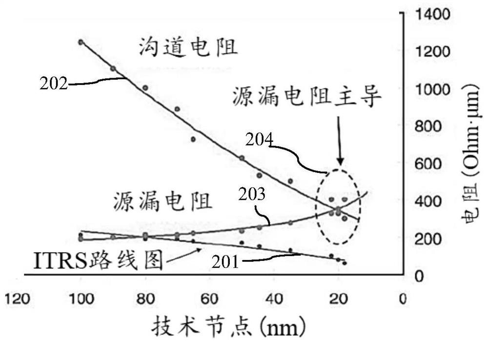
However, the premise of using this existing extraction method is to assume that the transistor channel is uniformly doped
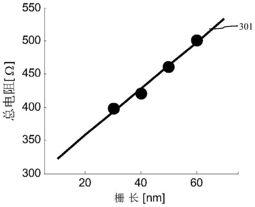
However, in short-channel devices, the halo effect in shallow doping technology, that is, the formation of the halo implantation region will cause uneven channel doping of the transistor, and the method of using the gate length array to extract the source-drain resistance will bring big error
Secondly, this method needs to design and layout several transistors with different channel lengths, which not only occupies the chip area, but also makes the test time doubled according to the transistor data, which is a waste of space and time
Finally, for a particular transistor, this method cannot extract the source-drain resistance of a single transistor

Method used


Image

  • Extraction method of source-drain resistance of field effect transistor
  • Extraction method of source-drain resistance of field effect transistor
  • Extraction method of source-drain resistance of field effect transistor

Examples


Embodiment Construction

[0069] like Figure 4 shown is a flowchart of a method for extracting source-drain resistance of a field effect transistor according to an embodiment of the present invention; Figure 5 shown are the first electrical characteristic curve and the third electrical characteristic curve obtained in the embodiment of the present invention; as Image 6 As shown, is the second relationship curve 502 obtained in the embodiment of the present invention; the method for extracting the source-drain resistance of the field effect transistor in the embodiment of the present invention includes the following steps:

[0070] Step 1: Test to obtain a first electrical characteristic curve 401 formed by the absolute value of the drain current and the gate voltage of the linear region of the field effect transistor.

[0071] Figure 5 , the drain current is I D Indicates that the gate voltage is represented by V G means that the ordinate of the first electrical characteristic curve 401 corresp...


PUM


Abstract

The invention discloses a method for extracting source-drain resistance of a field effect transistor, comprising the steps of: step 1: testing to obtain a first electrical characteristic curve formed by the absolute value of the drain current and the gate voltage of the linear region of the field effect transistor, and extracting the linear region threshold voltage; step 2, select multiple sampling points in the high grid voltage region, calculate the reciprocal of the absolute value of the difference between the grid voltage corresponding to each sampling point and the threshold voltage in the linear region and use it as the first parameter; step 3, calculate each sampling point The ratio of the drain voltage and the drain current is taken as the total resistance; step 4, form a second relationship curve according to the first parameter and total resistance of each sampling point; step 5, extend the second relationship curve and intersect it with the vertical axis, Take the intercept as the source-drain resistance. The invention can extract the source-drain resistance for a single transistor, and is suitable for field effect transistors with uniform or non-uniform channel doping, which not only saves the test area, but also improves the test speed and the resistance extraction precision.

Description

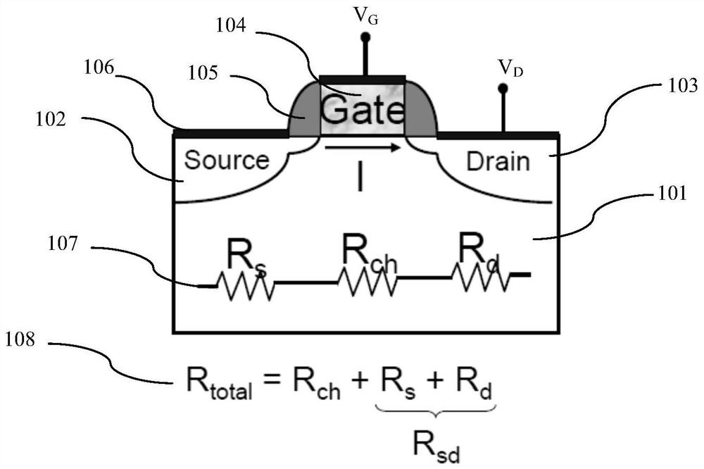
technical field [0001] The invention relates to a method for manufacturing a semiconductor integrated circuit, in particular to a method for extracting the source-drain resistance of a field effect transistor. Background technique [0002] like figure 1 Shown is a schematic diagram of the composition of the total resistance of the field effect transistor; the field effect transistor includes a source region 102 , a drain region 103 , a channel region and a gate structure 104 . figure 1 In the figure, the source region 102 is also represented by Source, the drain region 103 is also represented by Drain, and the gate structure 104 is also represented by Gate. [0003] The source region 102 and the drain region 103 are formed in the semiconductor substrate 101 on both sides of the gate structure 104, and the channel region is located between the source region 102 and the drain region 103 and is surrounded by The area covered by the gate structure 104 . [0004] The source re...

Claims


Application Information

Patent Timeline
Patent Type & Authority Patents(China)
IPC IPC(8): G01R27/08G01R31/26
CPCG01R27/08G01R31/2621
Inventor 李中华冷江华田明
Owner SHANGHAI HUALI INTEGRATED CIRCUIT CORP
Features
  • R&D
  • Intellectual Property
  • Life Sciences
  • Materials
  • Tech Scout
  • Unparalleled Data Quality
  • Higher Quality Content
  • 60% Fewer Hallucinations
Learn More