

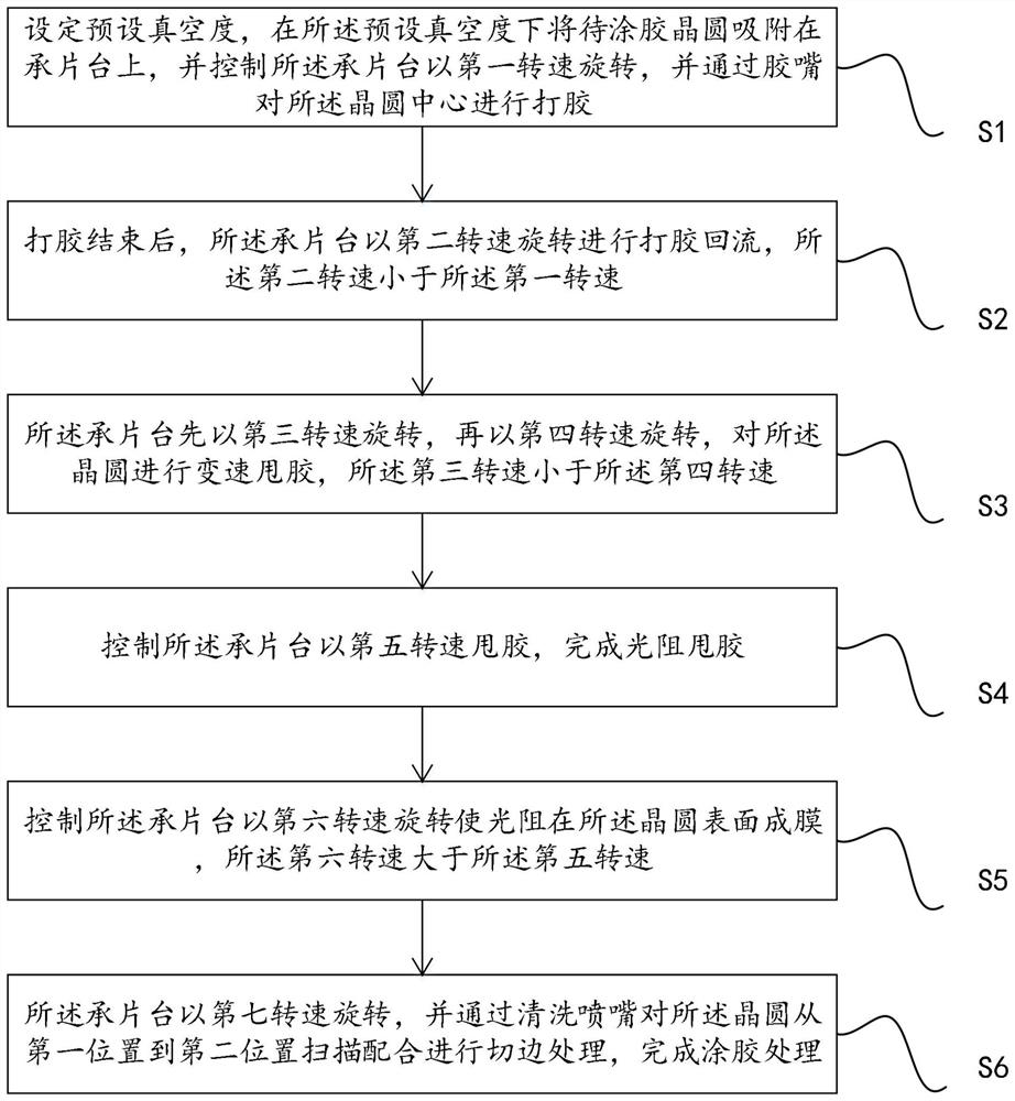
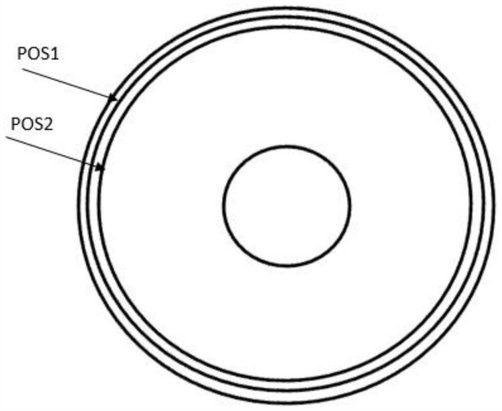
Gluing method for thinning-type wafer
A wafer and gluing technology, which is applied in coatings, devices for coating liquid on the surface, electrical components, etc. Glue accumulation and other problems, to achieve the effect of improving stability, good effect, and improving uniformity
- Summary
- Abstract
- Description
- Claims
- Application Information
AI Technical Summary
Problems solved by technology
Method used
Image

Examples
Embodiment 1
[0055] The photoresist coating is carried out on a wafer with a thickness of 50 μm and a diameter of 200 nm at the thinning part, and the photoresist viscosity value is 34 cp (centipoise), including the following steps:
[0056] S1a: Vacuum absorb the wafer onto the wafer stage, control the preset vacuum degree of the wafer stage to 40kpa, and the exhaust air volume in the glue chamber to be 30m / s, and the wafer stage is operated at the first high speed of 1000r / s Rotate for 10s, while the glue nozzle applies glue to the center of the wafer;
[0057] S2a: After the gluing is finished, the wafer carrier rotates at the first low speed of 100r / s for 5s to carry out gluing reflow;
[0058] S3a: the wafer carrier is rotated at a second low speed of 100r / s for 10s, and then rotated at a second high speed of 1500r / s for 5s to perform variable speed glue removal;
[0059] S4a: The wafer carrier is rotated at the third low speed of 100r / s for 5s to complete the removal of the photores...
Embodiment 2
[0064] The photoresist coating is carried out on a wafer with a thinning part of 80 μm and a diameter of 200 nm. The photoresist viscosity value is 34 cp (centipoise), including the following steps:
[0065] S1b: Vacuum absorb the wafer onto the wafer stage, control the preset vacuum degree of the wafer stage to 20kpa, and the exhaust air volume in the gluing chamber to 40m / s, and the wafer stage is operated at the first high speed of 800r / s Rotate for 10s, while the glue nozzle applies glue to the center of the wafer;
[0066] S2b: After the gluing is finished, the wafer carrier rotates at the first low speed of 100r / s for 5s to carry out gluing reflow;
[0067] S3b: The wafer carrier is rotated at a second low speed of 100r / s for 10s, and then rotated at a second high speed of 1600r / s for 5s to perform variable speed glue rejection;
[0068] S4b: The wafer carrier is rotated at a third low speed of 100r / s for 5s to complete photoresist rejection;
[0069] S5b: The wafer st...
Embodiment 3
[0073] Coating photoresist on a wafer with a thickness of 100 μm and a diameter of 200 nm at the thinning part, the viscosity of the photoresist is 34 cP (centipoise), including the following steps:
[0074] S1c: Vacuum absorb the wafer onto the wafer stage, control the preset vacuum degree of the wafer stage to 10kpa, and the exhaust air volume in the glue chamber to be 40m / s, and the wafer stage is operated at the first high speed of 700r / s Rotate for 10s, while the glue nozzle applies glue to the center of the wafer;
[0075] S2c: After the gluing is finished, the wafer carrier is rotated at the first low speed of 100r / s for 5s for gluing reflow;
[0076] S3c: the wafer carrier is rotated at the second low speed of 100r / s for 10s, and then rotated at the second high speed of 1700r / s for 5s to change the speed and reject the glue;
[0077] S4c: The wafer carrier is rotated at the third low speed of 100r / s for 5s to complete the removal of the photoresist;
[0078] S5c: the...
PUM
 Abstract
Description
Claims
Application Information