Electromagnetic metasurface design method and device based on deep learning
A technology of deep learning and design method, applied in the field of electromagnetic metamaterials, can solve problems such as the actual effect of defect design, theoretical effect, mismatch, etc., to achieve the effect of reducing computational complexity and shortening computational time
- Summary
- Abstract
- Description
- Claims
- Application Information
AI Technical Summary
Problems solved by technology
Method used
Image
Examples
Embodiment 1
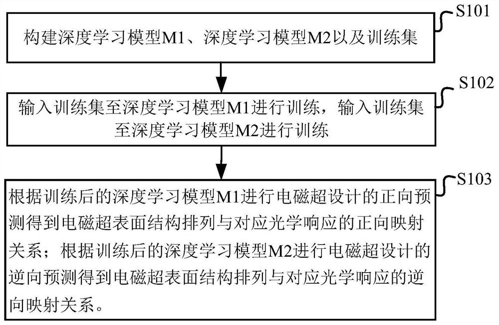
[0054] figure 1 shows a flow chart of the steps of a method for designing an electromagnetic metasurface based on deep learning according to an embodiment of the present application.
[0055] like figure 1 As shown, the deep learning-based electromagnetic metasurface design method of this embodiment specifically includes the following steps:
[0056] Step S101: Construct a deep learning model M1, a deep learning model M2 and a training set.
[0057] In S101, elements of the training set include incident wave information, electromagnetic metasurface structures / arrangements and corresponding optical responses.
[0058] Among them, the samples of the training set are obtained in the following way: First, the electromagnetic simulation software is used to simulate different electromagnetic metasurface structures / arrangements, and the corresponding optical response results are obtained. Then, the optical response results are combined with the electromagnetic metasurface structur...
Embodiment 2
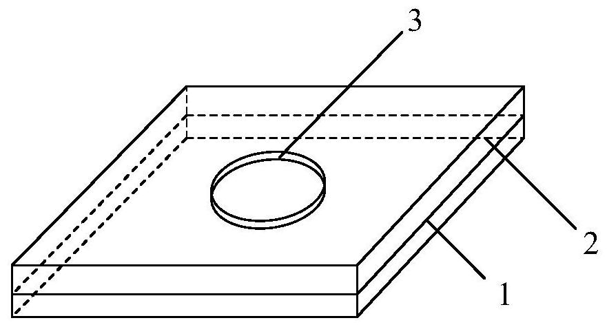
[0072] This embodiment provides an electromagnetic metasurface material. figure 2 A schematic structural diagram of an electromagnetic superunit of an electromagnetic metasurface according to an embodiment of the present application is shown in .
[0073] like figure 2 As shown, the electromagnetic superunit includes an upper dielectric layer 3, an intermediate dielectric layer 2, and a lower dielectric layer 1, specifically:
[0074] The upper dielectric layer 1 is fixed on the upper surface of the intermediate dielectric layer 2, and the upper dielectric layer 3 has a fully polarized resonance structure; the intermediate layer dielectric is a non-metallic layer 2; the lower dielectric layer 1 is a metal layer, and the upper surface of the lower dielectric layer 1 is connected to the The lower surface of the middle dielectric layer 2 is close to and completely matched.
[0075] Wherein, the metal resonant structure may be a metal pattern such as a circle, a ring, an I-sha...
Embodiment 3
[0079] The deep learning-based electromagnetic metasurface design method provided in this application is applicable to various models. This embodiment takes a simple flat model and a flying saucer model with a complex curved structure as examples.
[0080] image 3 A schematic diagram of the structure of a flat plate model covered with an electromagnetic metasurface according to an embodiment of the present application is shown in . Figure 4 shows a schematic structural diagram of a flying saucer model covered with an electromagnetic metasurface according to an embodiment of the present application.
[0081] Figure 5 A flow chart of a method for designing an electromagnetic metasurface based on deep learning according to Embodiment 3 of the present application is shown.
[0082] The present invention is described in further detail with the flying saucer model that is covered with electromagnetic metasurface, as Figure 5 As shown, firstly, step S1 is performed to construc...
PUM
 Abstract
Description
Claims
Application Information


