Wafer and wafer testing method

A testing method and wafer testing technology, applied in semiconductor/solid-state device testing/measurement, electrical components, electrical solid-state devices, etc., can solve the problem of reduced utilization of wafer testing machines and incompatibility testing of traditional wafers and wafers Increased test costs and other issues, to achieve the effect of providing versatility and utilization, multiple times of reuse, and reducing the risk of wafer damage

Pending Publication Date: 2020-09-01
SIEN QINGDAO INTEGRATED CIRCUITS CO LTD
View PDF5 Cites 0 Cited by
  • Summary
  • Abstract
  • Description
  • Claims
  • Application Information

AI Technical Summary

Problems solved by technology

This method of changing the vacuum chuck involves equipment modification, which will inevitably increase the cost of testing, and it cannot be restored at zero cost after the modification, so it cannot be compatible with testing traditional wafers
As a result, the utilization rate of wafer testing equipment is reduced, and the cost of wafer testing is increased

Method used


Image

  • Wafer and wafer testing method
  • Wafer and wafer testing method
  • Wafer and wafer testing method

Examples


Embodiment 1

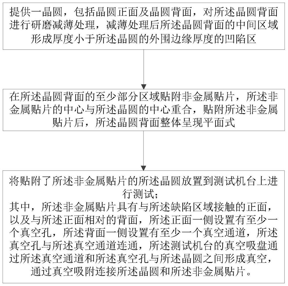
[0092] In order to overcome the problems such as the low utilization rate of the wafer test machine and the increase of test cost caused by the equipment transformation done for testing the Taiko wafer in the prior art, the present embodiment provides a wafer test method, such as image 3 As shown, the method includes the following steps:

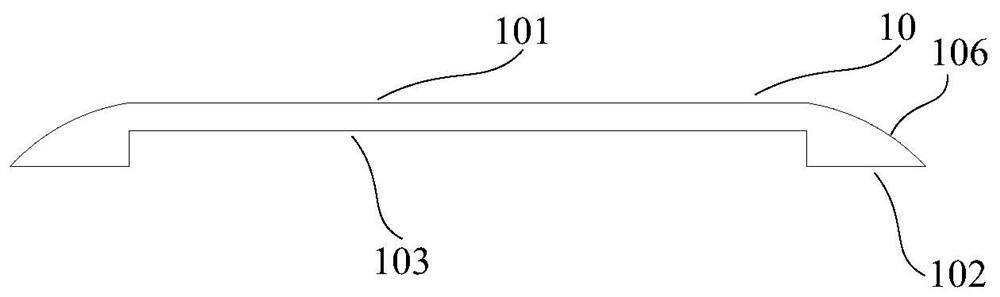
[0093] A wafer is provided, including a wafer front and a wafer back, and the back of the wafer is ground and thinned. After the thinning, the middle area of ​​the back of the wafer is formed with a thickness smaller than that of the peripheral edge of the wafer. depressed area;

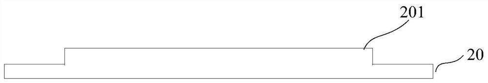
[0094] A non-metallic patch is attached to at least part of the area on the back of the wafer, the center of the non-metallic patch coincides with the center of the wafer, and after the non-metallic patch is attached, the entire back of the wafer present a flat form;

[0095] placing the wafer attached with the non-metal patch on a testing machine for testing; ...

Embodiment 2

[0108] This embodiment also provides a wafer testing method, and the similarities with Embodiment 1 will not be repeated, but the differences are:

[0109] Such as Figure 9 As shown, the wafer 90 provided in this embodiment has a wafer front 901 and a wafer back 902 , and the middle area of ​​the wafer back 902 has a recessed area 903 . The backside 902 of the wafer is attached with a non-metal patch 60 . Such as Figure 10 As shown, the non-metallic patch 60 has a front surface 601 in contact with the wafer backside 902 of the wafer 90 and a backside 602 opposite to the real surface 601. The nonmetallic patch 60 includes a cylindrical bottom 61 and a bottom surface along the bottom. 607 extends upwardly in a direction perpendicular to the bottom 607 to form a cylindrical protrusion 606 . In this embodiment, the protruding portion 606 fills the recessed area 903 on the backside of the wafer 90 . still refer to Figure 10 and combine as Figure 11 and 12 As shown, in th...

Embodiment 3

[0114] This embodiment provides a wafer, including a wafer, the wafer has a wafer front and a wafer back, the middle area of ​​the wafer back has a recessed area, and the thickness of the recessed area is smaller than that of the wafer. peripheral edge thickness; and

[0115] A non-metallic patch attached to at least a partial area of ​​the backside of the wafer, the center of the metal patch coincides with the center of the wafer, and after the metal patch is attached, the backside of the wafer presents an overall Plane;

[0116] Wherein, the metal patch has a front surface in contact with the defect area, and a back surface opposite to the front surface, at least one vacuum hole is provided on one side of the front surface, and at least one vacuum channel is provided on the back side, The vacuum hole communicates with the vacuum channel.

[0117] In another preferred embodiment of this embodiment, the backside of the wafer further includes a thin metal layer formed by gold...


PUM


Abstract

The invention provides a wafer and a wafer testing method, and the method comprises the following steps of providing the wafer which comprises a wafer front surface and a wafer back surface; attachinga non-metal patch to at least part of the region of the back surface of the wafer; and placing the wafer to which the non-metal patch is attached on a test machine for testing. The non-metal patch isattached to the back surface of the wafer, so that the strength of the wafer can be improved, the warping phenomenon of the wafer is effectively prevented, and meanwhile, the risk of wafer damage inthe carrying process can be reduced. The back surface of the wafer attached with the non-metal patch is integrally planar, so that the wafer with a concave area on the back surface of the wafer can bedirectly placed on a chuck or a sucker of a traditional testing machine for testing, the equipment transformation cost is saved, the universality and the utilization rate of the testing machine are improved, and the wafer testing cost is reduced. The filled non-metal patches are recycled after the test is completed, and the non-metal patches can be repeatedly used, so that the testing cost of thewafer is further reduced.

Description

technical field [0001] The invention relates to the technical field of integrated circuits, in particular to the field of semiconductor power device manufacturing, and more specifically to a wafer and a wafer testing method. Background technique [0002] In integrated circuits, power devices are an important application area. In the manufacturing process of power devices, the backside process of the wafer has an important impact on the reduction of device resistance and subsequent packaging. For the grinding process of the backside process, there are mainly TAIKO process and non-TAIKO traditional grinding process in the prior art. When the wafer is ground by the TAIKO process, the outer edge of the wafer will be retained, and only the inside of the wafer will be ground and thinned. This process can reduce the handling risk of thin wafers, and can reduce the warpage of wafers caused by traditional grinding processes, and improve the strength of wafers. [0003] However, si...

Claims


Application Information

Patent Timeline
Patent Type & Authority Applications(China)
IPC IPC(8): H01L21/66H01L21/683
CPCH01L22/12H01L21/6838H01L21/6835H01L2221/6834
Inventor 管振兴严大生蔡育源徐传贤司徒道海
Owner SIEN QINGDAO INTEGRATED CIRCUITS CO LTD
Why Eureka
Try Eureka