Mask, method for preparing semiconductor device and semiconductor device

A mask and semiconductor technology, applied in the semiconductor field, can solve the problems of left side deviation of size, influence of gold bump preparation accuracy, increase of manufacturing cost, etc., and achieve the effects of compensating for deformation, saving preparation cost, and improving preparation accuracy

Active Publication Date: 2020-09-08
厦门通富微电子有限公司
View PDF4 Cites 0 Cited by
  • Summary
  • Abstract
  • Description
  • Claims
  • Application Information

AI Technical Summary

Problems solved by technology

Obviously, when using the patterned photoresist layer 202 to prepare gold bumps, such as Figure 3 and Figure 4 As shown in , when gold bumps 204 are formed by electroplating into each opening window 201, and the rest of the photoresist layer 202 is etched to finally obtain the finished gold bumps 204, the leftmost gold bump There is an obvious deviation on the left side of the 204 size, which affects the preparation accuracy of the gold bumps. In addition, if the expected gold bumps are formed by filling metal materials in the later stage, the leftmost gold bumps need to use more than the design requirements. Filling with metal materials will increase material consumption and increase manufacturing costs

Method used


Image

  • Mask, method for preparing semiconductor device and semiconductor device
  • Mask, method for preparing semiconductor device and semiconductor device
  • Mask, method for preparing semiconductor device and semiconductor device

Examples


Embodiment Construction

[0039] In order to enable those skilled in the art to better understand the technical solution of the present disclosure, the present disclosure will be described in further detail below in conjunction with the accompanying drawings and specific embodiments.

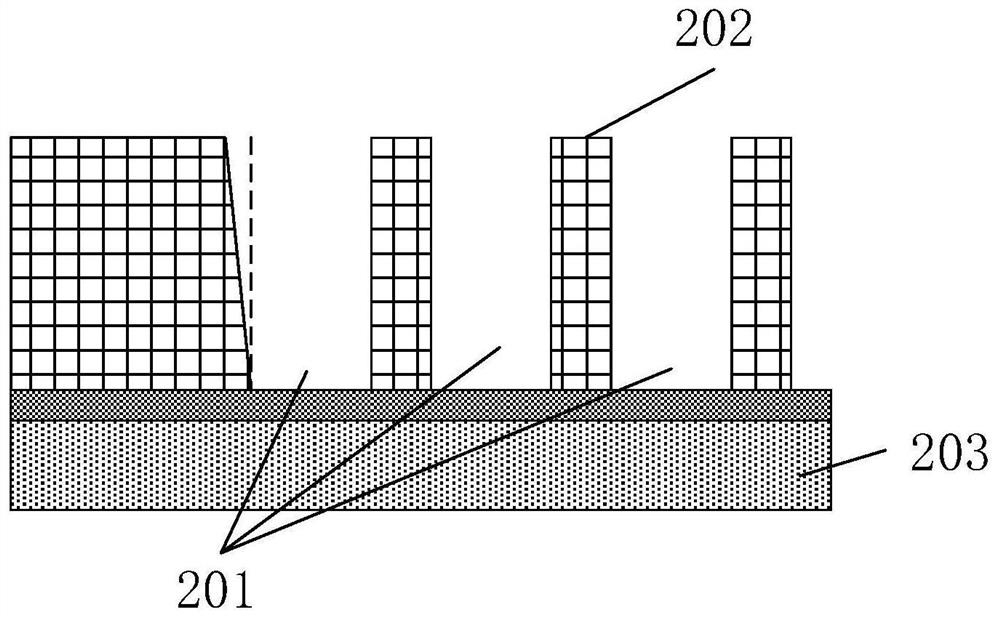
[0040] Such as Figure 5 As shown, it is a mask plate 300 proposed in this embodiment, the mask plate 300 includes a mask substrate 307, and the mask substrate 307 is along its first predetermined direction A, and the first predetermined direction A can be For the length direction or width direction of the mask substrate 307, a plurality of first regions 301 for forming target patterns and a second region 302 surrounding the plurality of first regions 301 are arranged at intervals, and the first regions 301 One of the second area 301 and the second area 302 is a light-shielding area, and the other of the first area 301 and the second area 302 is a light-transmitting area. The specific types of the first area 301 and the ...


PUM


Abstract

The invention provides a mask, a method for preparing a semiconductor device and the semiconductor device. The mask comprises a mask substrate, the mask substrate is provided with a plurality of firstareas used for forming a target graph and arranged at intervals in a first preset direction and a second area arranged around the first areas, one of the first areas and the second area is a shadingarea, and the other one of the first areas and the second area is a light transmitting area; wherein at least one target first area exists in the plurality of first areas, and at least one side of thetarget first area meets the condition that the rest of the first areas do not exist in a preset distance threshold value along the first preset direction. The embodiment of the invention provides a new mask structure, the windowing pattern of the non-uniform and non-tight area in the mask is subjected to shrinkage design, and in a baking process, the shape of the shrinkage pattern after being heated to expand outwards is the same as that of the original design, the preparation precision of the semiconductor device is improved, and the preparation cost is saved.

Description

technical field [0001] The disclosure belongs to the technical field of semiconductors, and in particular relates to a mask, a method for preparing a semiconductor device and a semiconductor device. Background technique [0002] In the existing semiconductor devices, such as the process of gold bumps, the photoresist layer coated on the wafer is generally exposed and developed through a designed mask to obtain an open photoresist layer. After that, metal material is filled into the opening to form a gold bump. [0003] Such as figure 1 As shown, it is a schematic diagram of a traditional mask structure. The mask 100 includes a plurality of light-shielding regions 101 and light-transmitting regions 102 arranged at intervals. figure 1 , the left side of the leftmost light-shielding area 101 is an open area (there are no other light-shielding areas 101). Like this, when utilizing the mask plate 100 of this structure to pattern the photoresist layer, combine together figure...

Claims


Application Information

Patent Timeline
Patent Type & Authority Applications(China)
IPC IPC(8): G03F1/00
CPCG03F1/00
Inventor 陈运生
Owner 厦门通富微电子有限公司
Why Eureka
Try Eureka