Memory and method of forming the same

A memory and bit line technology, which is applied in the manufacture of semiconductor devices, electrical solid state devices, semiconductor/solid state devices, etc., can solve problems such as abnormal appearance and impact on memory performance, to ensure appearance, improve appearance accuracy, and improve device performance. performance effect

Active Publication Date: 2022-03-25
FUJIAN JINHUA INTEGRATED CIRCUIT CO LTD
View PDF2 Cites 0 Cited by
  • Summary
  • Abstract
  • Description
  • Claims
  • Application Information

AI Technical Summary

Problems solved by technology

[0005] The purpose of the present invention is to provide a memory to solve the problem that the bit line and node contact at the edge of the existing memory are prone to abnormal morphology, thereby affecting the performance of the memory

Method used


Image

  • Memory and method of forming the same
  • Memory and method of forming the same
  • Memory and method of forming the same

Examples


Embodiment 2

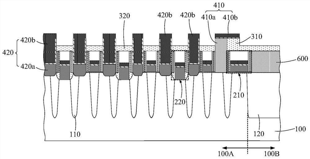
[0152] The difference from the first embodiment is that, in this embodiment, a third contact portion and a fourth contact portion are further provided in the peripheral region. Figure 5 It is a schematic cross-sectional view of the memory in the second embodiment of the present invention, such as Figure 5 As shown, the third contact portion 430 includes an insulating pillar 430a and a third electrically conductive layer 430b, and the third electrically conductive layer 430b covers the top surface of the insulating pillar 430a. Also, the fourth contact portion 440 only includes insulating pillars.

[0153] Further, the fourth contact portions 440 and the third contact portions 430 are alternately arranged in sequence, and isolation is also filled between the insulating pillars 430a of the third contact portion 430 and the insulating pillars of the fourth contact portion 440 Material. In this embodiment, a fourth contact portion 440 is spaced between the third contact portio...


PUM


Abstract

The present invention provides a memory and a method of forming the same. By making the width dimension of the first bit line located at the edge position in the bit line group larger than the width dimension of the second bit line arranged in the bit line group, when the bit line group is prepared, not only the morphology of the first bit line can be guaranteed, but also the shape of the first bit line can be guaranteed. In addition, under the blocking protection of the first bit line with a larger width, the topography accuracy of the second bit line can also be improved, which is beneficial to improve the device performance of the formed memory. Similarly, since the width dimension of the first contact portion located at the edge position among the plurality of node contact portions is larger than the width dimension of the second contact portion, the topography of the first contact portion can be guaranteed correspondingly, and the pattern of the second contact portion can be improved accordingly. accuracy, further improving the device performance of the formed memory.

Description

technical field [0001] The present invention relates to the technical field of semiconductors, and in particular, to a memory and a method for forming the same. Background technique [0002] A memory, such as a dynamic random access memory (DRAM), usually has a memory cell array, and the memory cell array includes a plurality of memory cells arranged in an array. And, the memory also has a plurality of bit lines, each of which is electrically connected to a corresponding storage unit, and the memory further includes a storage capacitor for storing charges representing stored information, and all The storage unit can be electrically connected to the storage capacitor through a node contact portion, so as to realize the storage function of each storage unit. [0003] At present, a method for forming a memory generally includes: forming a bit line group, and using the bit line group to define a node contact window, and then filling the node contact window with a conductive mat...

Claims


Application Information

Patent Timeline
Patent Type & Authority Patents(China)
IPC IPC(8): H01L27/108H01L21/768H01L23/528H01L21/8242
CPCH10B12/312H10B12/30
Inventor 赖惠先林昭维朱家仪童宇诚吕前宏
Owner FUJIAN JINHUA INTEGRATED CIRCUIT CO LTD
Why Eureka
Try Eureka