Supercharge Your Innovation With Domain-Expert AI Agents!

Printed circuit board (PCB) copper foil edge cutting and board-splitting integrated equipment and PCB copper foil edge cutting and board-splitting process method

A technology of split-board integration and PCB board, which is applied in lighting and heating equipment, shearing machine equipment, metal processing equipment, etc., can solve the problems of high labor intensity, restrict production efficiency, increase enterprise cost, etc., and achieve the improvement of factory automation procedures, The effect of reducing labor intensity and improving production efficiency

Pending Publication Date: 2020-10-02
苏州威邦自动化机械有限公司
View PDF0 Cites 2 Cited by
  • Summary
  • Abstract
  • Description
  • Claims
  • Application Information

AI Technical Summary

Problems solved by technology

[0003] 1. Waste of resources, increasing costs: Copper foil is a huge consumption and cost item in the PCB production process. Some PCB manufacturers do not cut and recycle the excess copper foil edges of PCB boards for production efficiency, which greatly wastes resources. and increased business costs
[0004] 2. Low work efficiency: Nowadays, when PCB boards are printed, it is common to manually cut the copper foil and divide the board, and the general cutting process line has a harsh environment and high labor intensity. Repeated manual work is prone to fatigue, and then It will restrict production efficiency, thereby affecting the benefits of the factory, and is not conducive to improving the market competitiveness of enterprises
[0005] 3. Affect the automation of the entire PCB industry, which is not conducive to the advancement of factory intelligence

Method used

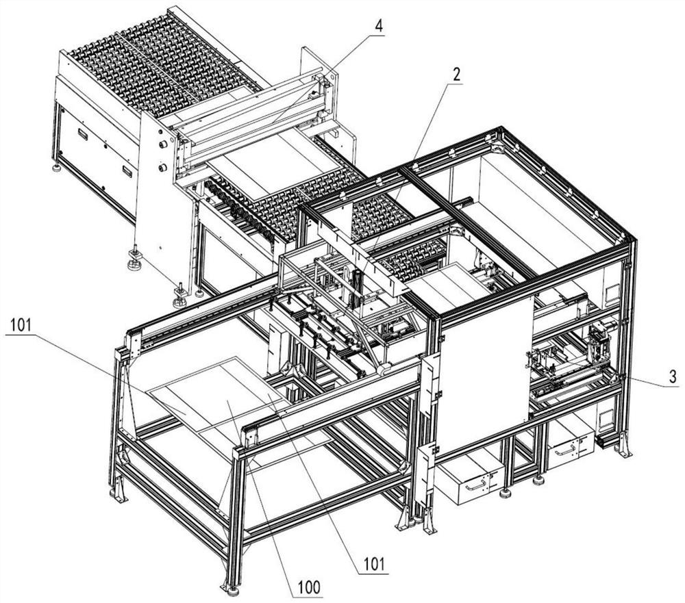
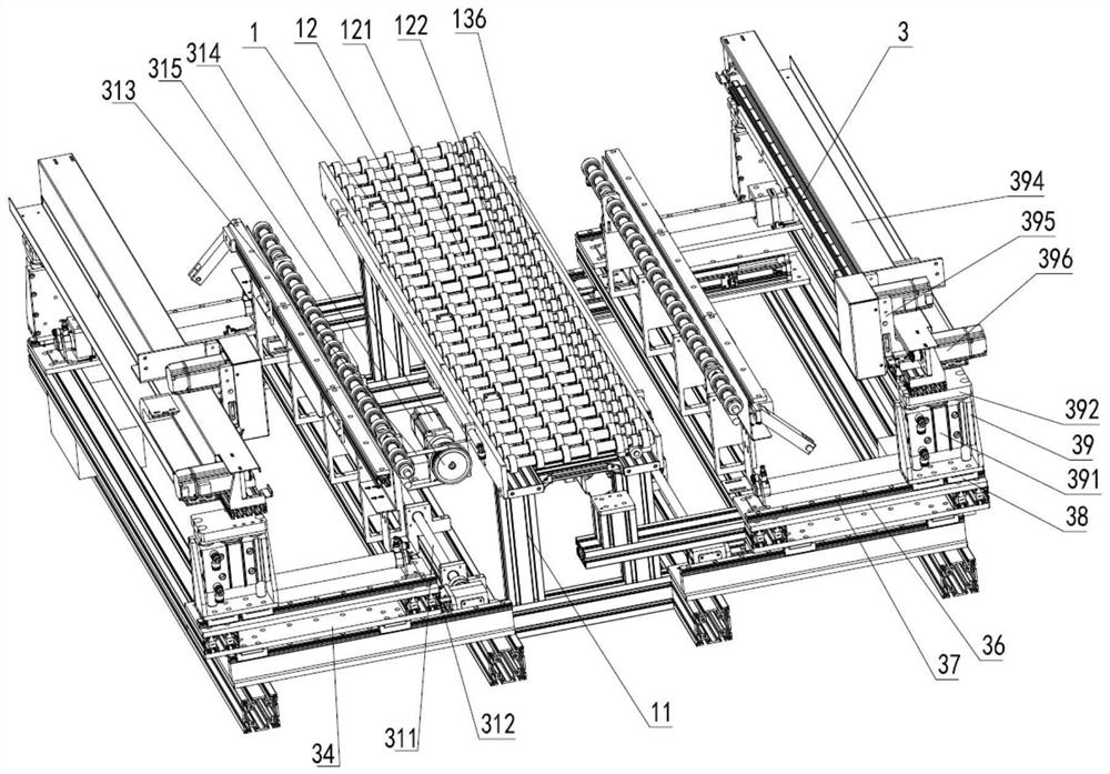

Image

  • Printed circuit board (PCB) copper foil edge cutting and board-splitting integrated equipment and PCB copper foil edge cutting and board-splitting process method
  • Printed circuit board (PCB) copper foil edge cutting and board-splitting integrated equipment and PCB copper foil edge cutting and board-splitting process method
  • Printed circuit board (PCB) copper foil edge cutting and board-splitting integrated equipment and PCB copper foil edge cutting and board-splitting process method

Examples


Embodiment Construction

[0046] The present invention will be described in detail below in conjunction with specific embodiments shown in the accompanying drawings. However, these embodiments are not limited to the present invention, and structural, method, or functional changes made by those skilled in the art according to these embodiments are included within the protection scope of the present invention.

[0047] In describing the present invention, it should be understood that the terms "center", "longitudinal", "transverse", "upper", "lower", "front", "rear", "left", "right", " The orientations or positional relationships indicated by "vertical", "horizontal", "top", "bottom", "inner" and "outer" are based on the orientations or positional relationships shown in the drawings, and are only for the convenience of describing the present invention and Simplified descriptions, rather than indicating or implying that the device or element referred to must have a particular orientation, be constructed a...


PUM


Abstract

The invention discloses printed circuit board (PCB) copper foil edge cutting and board-splitting integrated equipment and a PCB copper foil edge cutting and board-splitting process method. The PCB copper foil edge cutting and board-splitting integrated equipment comprises a bearing and conveying assembly for bearing and conveying PCBs, an adsorption assembly for adsorbing the PCBs and placing thePCBs on the bearing and conveying assembly is arranged above the conveying assembly, and the motion direction of the adsorption assembly is spatially perpendicular to the motion direction of the bearing and conveying assembly; cutting assemblies which are of symmetrical structures and are used for cutting copper foil edges on the two sides of the PCBs are arranged on the two sides of the bearing and conveying assembly; and a shearing assembly closely attached to the bearing and conveying assembly for shearing the PCBs with the copper foil edges on the two sides being removed is further arranged on one side in the motion direction of the bearing and conveying assembly. The PCB copper foil edge cutting and board-splitting integrated equipment and the PCB copper foil edge cutting and board-splitting process method have the beneficial effects mainly embodied in that the structure is exquisite, fully-automatic conveying of the PCBs, copper foil edge cutting and automatic precise board-splitting of the PCBs are realized, the production efficiency is improved, the automation program of a factory is improved, the labor intensive degree is decreased, the production cost is lowered, and construction of an intelligent factory is facilitated.

Description

technical field [0001] The present invention relates to the field of PCB production, in particular to a PCB copper foil cutting and board-splitting integrated equipment and a process method thereof. Background technique [0002] At present, there is no fully automated equipment for the dismantling process after PCB board lamination, and most of them are manually operated to realize the recycling of excess copper foil trimming, the division of multi-panel boards, and even some production process lines do not cut excess copper at all. Foil edges, the defects of which are as follows: [0003] 1. Waste of resources, increasing costs: Copper foil is a huge consumption and cost item in the PCB production process. Some PCB manufacturers do not cut and recycle the excess copper foil edges of PCB boards for production efficiency, which greatly wastes resources. And increased business costs. [0004] 2. Low work efficiency: Nowadays, when PCB boards are printed, it is common to manu...

Claims


Application Information

Patent Timeline
IPC IPC(8): B23D31/00B23D33/02B65G49/06
CPCB23D31/002B23D33/02B65G49/061
Inventor 徐齐孝李晨
Owner 苏州威邦自动化机械有限公司
Features
  • R&D
  • Intellectual Property
  • Life Sciences
  • Materials
  • Tech Scout
  • Unparalleled Data Quality
  • Higher Quality Content
  • 60% Fewer Hallucinations
Learn More