Semiconductor device and forming method thereof

A technology of semiconductors and devices, which is applied in the field of semiconductor devices and their formation, and can solve the problems that the suspended part of the passivation layer is prone to damage, etc.

Active Publication Date: 2020-10-02
SEMICON MFG ELECTRONICS (SHAOXING) CORP
View PDF10 Cites 3 Cited by
  • Summary
  • Abstract
  • Description
  • Claims
  • Application Information

AI Technical Summary

Problems solved by technology

[0009] The object of the present invention is to provide a method for forming a semiconductor device, so as to solve the problem that the floating part of the passivation layer is easily damaged in the existing forming method

Method used


Image

  • Semiconductor device and forming method thereof
  • Semiconductor device and forming method thereof
  • Semiconductor device and forming method thereof

Examples


Embodiment Construction

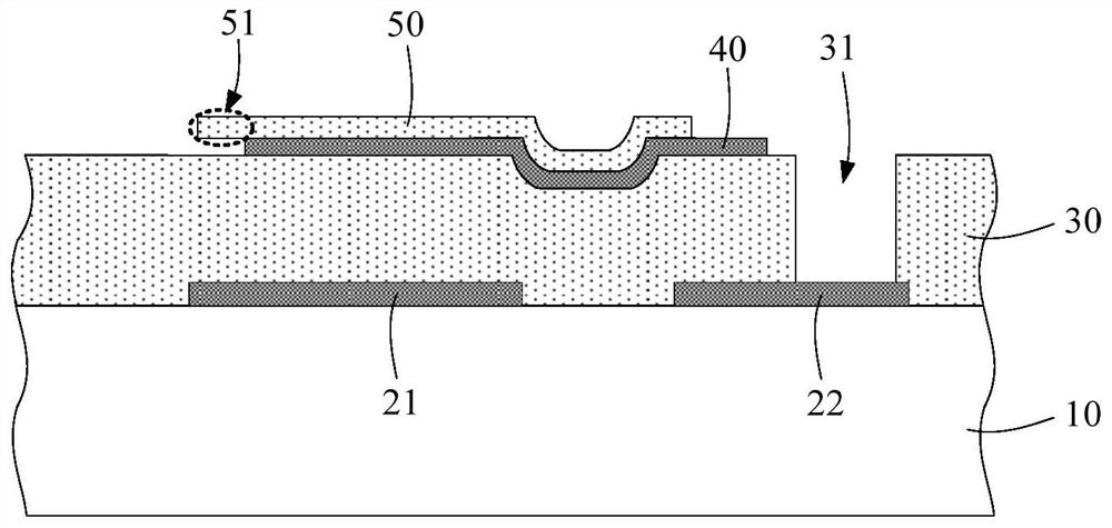
[0053] As mentioned in the background, in the current manufacturing method of semiconductor devices, when the photoresist layer is removed based on high-intensity spraying pressure, the suspended part of the passivation layer is easily damaged. Based on this, even if the spraying pressure is reduced to avoid the damage of the suspended part, however, the photoresist layer will not be completely removed at this time.

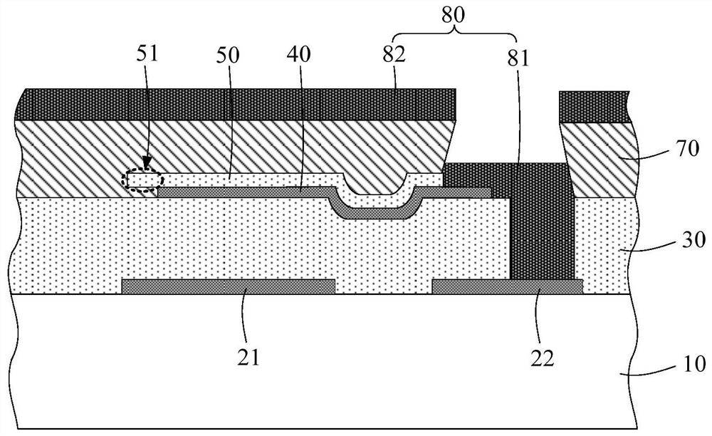
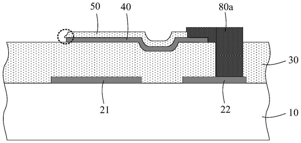
[0054]Therefore, the present invention provides a method for forming a semiconductor device, so as to ensure that the photoresist layer can be completely removed and prevent the problem of damage to the floating portion in the passivation layer. For example reference figure 2 As shown, the forming method of the semiconductor device includes:

[0055] Step S100, providing a substrate, on which a lower electrode layer and an extraction electrode are formed, and a piezoelectric material layer, an upper electrode layer, and a passivation layer are sequentially form...


PUM


Abstract

The invention provides a semiconductor device and a forming method thereof. A protective layer is formed between a photoresist layer and a passivation layer, so that a film layer below the protectivelayer can be prevented from being damaged under the interval protection of the protective layer. Specifically, the passivation layer can be prevented from being exposed when the photoresist layer is stripped, so that a suspension part in the passivation layer can be prevented from being damaged, on one hand, the size of the suspension part in the passivation layer can be further increased to improve the performance of the device, and on the other hand, the spraying pressure of the stripping liquid can be further increased when the photoresist layer is removed to improve the stripping efficiency of the photoresist layer and improve the problem that the photoresist layer cannot be removed completely.

Description

technical field [0001] The invention relates to the technical field of semiconductors, in particular to a semiconductor device and a forming method thereof. Background technique [0002] Semiconductor devices made using the inverse piezoelectric effect of piezoelectric materials are key components of crystal oscillators and filters, and are often used in bulk acoustic wave filters. Figure 1a ~ Figure 1c It is a schematic diagram of the structure of a semiconductor device in its fabrication process, such as Figure 1a ~ Figure 1c As shown, the method for forming the semiconductor device may include the following steps. [0003] Step 1, specific reference Figure 1a As shown, a substrate 10 is provided, on which a lower electrode layer 21 , a piezoelectric material layer 30 , an upper electrode layer 40 and a passivation layer 50 are sequentially formed. [0004] Wherein, the passivation layer 50 also has a suspended portion 51 extending from the upper electrode layer 40 , a...

Claims


Application Information

Patent Timeline
Patent Type & Authority Applications(China)
IPC IPC(8): H01L41/053H01L41/23H03H9/54
CPCH03H9/54H10N30/883H10N30/02
Inventor 穆苑龙项少华王冲王大甲魏有晨王俊力
Owner SEMICON MFG ELECTRONICS (SHAOXING) CORP
Why Eureka
Try Eureka