A method for realizing no mode hopping in semiconductor laser chip wave locking

A technology of lasers and semiconductors, which is applied in the field of fiber lasers and semiconductors, can solve problems such as inability to lock waves and jump membranes, and achieve the effects of solving membrane jumps, eliminating stress, and improving heat dissipation performance

Active Publication Date: 2021-10-22
XIAN LIXIN PHOTOELECTRIC SCI & TECH
View PDF13 Cites 0 Cited by
  • Summary
  • Abstract
  • Description
  • Claims
  • Application Information

AI Technical Summary

Problems solved by technology

[0005] The purpose of the present invention is to solve the phenomenon of film jumping in the spectrum of the existing single-tube chip, and this phenomenon will cause the problem that the wave cannot be locked during the VBG wave locking process, and provide a method for realizing no mode hopping in the wave locking of the semiconductor laser chip

Method used


Image

  • A method for realizing no mode hopping in semiconductor laser chip wave locking
  • A method for realizing no mode hopping in semiconductor laser chip wave locking
  • A method for realizing no mode hopping in semiconductor laser chip wave locking

Examples


Embodiment 1

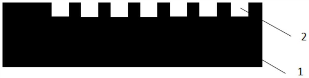
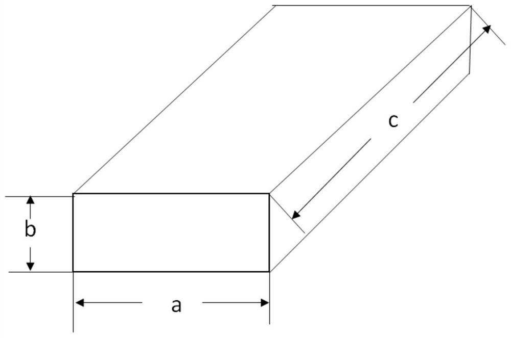
[0042] Such as image 3 As shown, the auxiliary heat sink is a cuboid (a×b×c), such as Figure 4 As shown, the groove design is performed on the surface of COS mounting (the upper surface composed of side a and side c), the groove is a linear groove, and the direction of the groove is parallel to side a.

Embodiment 2

[0044] Such as Figure 5 As shown, the groove is designed on the surface of COS mounting (the upper surface composed of side a and side c). The groove is a linear groove, and the direction of the groove is parallel to side c.

Embodiment 3

[0046] Such as Figure 6 As shown, the groove design is carried out on the surface of COS mounting (the upper surface composed of side a and side c). The groove is a linear groove, and the direction of the groove is parallel to sides a and c.


PUM


Abstract

The invention provides a method for realizing no mode-hopping in the wave-locking of a semiconductor laser chip, and solves the phenomenon of film-hopping in the spectrum of the existing single-tube chip, and this phenomenon will cause the problem that the wave-locking cannot be performed during the VBG wave-locking process. The method of the present invention includes the following steps: step 1, setting a plurality of grooves on the upper surface of the auxiliary heat sink, and the plurality of grooves are equidistantly arranged; step 2, mounting the ceramic heat sink with a single-tube chip on the auxiliary heat sink The upper surface of the heat sink; step 3, installing the auxiliary heat sink on the components of the optical fiber. At the same time, the mode-hop-free semiconductor laser of the present invention includes a single-tube chip, a ceramic heat sink, and an auxiliary heat sink that are stacked in sequence. The surface of the auxiliary heat sink and the ceramic heat sink is provided with multiple grooves, and the multiple grooves distance setting. The method of the present invention carries out groove design on the auxiliary heat sink, and the groove can release stress when the COS is mounted on the auxiliary heat sink to obtain a better spectrum, and then VBG wave locking can be performed.

Description

technical field [0001] The invention belongs to the field of semiconductors and fiber lasers, and in particular relates to a method for realizing no mode hopping in wave locking of semiconductor laser chips. Background technique [0002] Fiber lasers are widely used in laser optical fiber communication, industrial shipbuilding, industrial shipbuilding, automobile manufacturing, laser engraving, laser marking, laser cutting, printing roll making, metal and non-metal drilling / cutting / welding, etc. With the development of modernization, semiconductor lasers have gradually become the main pump source of fiber lasers. There are two types of semiconductor laser chips: bar and single-tube, and high-power single-tube chips have gradually become the main pump source of fiber lasers with the development of technologies such as space beam combining, wavelength beam combining and polarization beam combining. [0003] The packaging of the high-power semiconductor laser single-tube chip ...

Claims


Application Information

Patent Timeline
Patent Type & Authority Patents(China)
IPC IPC(8): H01S5/024
CPCH01S5/02469
Inventor 任占强李青民王宝超孙翔李喜荣仇伯仓
Owner XIAN LIXIN PHOTOELECTRIC SCI & TECH
Why Eureka
Try Eureka