Light-emitting display device and preparation method thereof and display device
A technology for light-emitting display devices and light-emitting layers, which is applied in semiconductor/solid-state device manufacturing, electric solid-state devices, semiconductor devices, etc., and can solve problems that can no longer meet the needs
- Summary
- Abstract
- Description
- Claims
- Application Information
AI Technical Summary
Problems solved by technology
Method used
Image

Examples
Embodiment 1
[0044] A method for preparing a light-emitting display device, comprising:
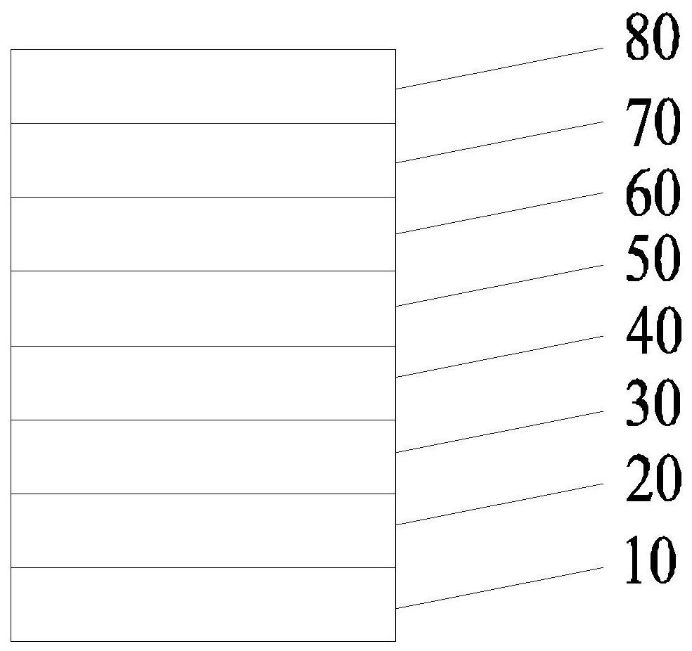
[0045] Under the condition that the degree of vacuum is 1×10⁻⁵Pa, an anode is formed on the glass substrate, the material of the anode is indium tin oxide (ITO), and the film thickness of the anode is 100nm;
[0046] The compound 1 is vapor-deposited on the anode by a vacuum evaporation method, so that the compound 1 forms a hole injection layer, and the film thickness of the hole injection layer is 5 nm;
[0047] By vacuum evaporation, compound 2 is evaporated on the hole injection layer, so that compound 2 forms a hole transport layer, and the film thickness of the hole transport layer is 50nm;
[0048] Compound A and compound B were co-evaporated on the hole transport layer by vacuum evaporation method, so that compound A and compound B formed a light-emitting layer, and the film thickness of the light-emitting layer was 35 nm. The mass percentage of compound A in the light-emitting layer is 50%, ...
Embodiment 2
[0057] An embodiment of the present invention provides a method for manufacturing a light-emitting display device, including:
[0058] Under the condition that the degree of vacuum is 1×10⁻⁵Pa, an anode is formed on the glass substrate, the material of the anode is indium tin oxide (ITO), and the film thickness of the anode is 100nm;
[0059] The compound 1 is vapor-deposited on the anode by a vacuum evaporation method, so that the compound 1 forms a hole injection layer, and the film thickness of the hole injection layer is 5 nm;
[0060] By vacuum evaporation, compound A is vapor-deposited on the hole injection layer, so that compound A forms a hole transport layer, and the film thickness of the hole transport layer is 50nm;
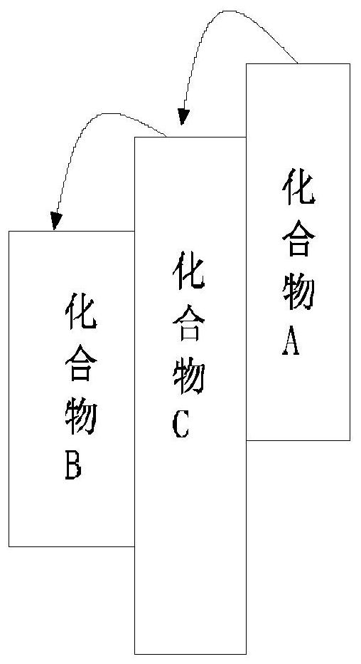
[0061] Compound A, compound B, and compound C were co-evaporated on the hole transport layer by vacuum evaporation, so that compound A, compound B, and compound C formed a light-emitting layer, and the film thickness of the light-emitting layer was 35 ...
Embodiment 3
[0070] An embodiment of the present invention provides a method for manufacturing a light-emitting display device, including:
[0071] Under the condition that the degree of vacuum is 1×10⁻⁵Pa, an anode is formed on the glass substrate, the material of the anode is indium tin oxide (ITO), and the film thickness of the anode is 100nm;
[0072] The compound 1 is vapor-deposited on the anode by a vacuum evaporation method, so that the compound 1 forms a hole injection layer, and the film thickness of the hole injection layer is 5 nm;
[0073] By vacuum evaporation, compound 2 is evaporated on the hole injection layer, so that compound 2 forms a hole transport layer, and the film thickness of the hole transport layer is 50nm;
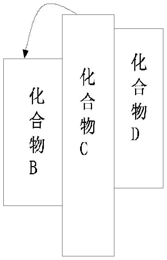
[0074] Compound A, compound B, and compound C were co-evaporated on the hole transport layer by vacuum evaporation, so that compound A, compound B, and compound C formed a light-emitting layer, and the film thickness of the light-emitting layer was 35 nm. ...
PUM
| Property | Measurement | Unit |
|---|---|---|
| thickness | aaaaa | aaaaa |
| thickness | aaaaa | aaaaa |
| thickness | aaaaa | aaaaa |
Abstract
Description
Claims
Application Information
 - R&D
- Intellectual Property
- Life Sciences
- Materials
- Tech Scout
- Unparalleled Data Quality
- Higher Quality Content
- 60% Fewer Hallucinations
Browse by: Latest US Patents, China's latest patents, Technical Efficacy Thesaurus, Application Domain, Technology Topic, Popular Technical Reports.
© 2025 PatSnap. All rights reserved.Legal|Privacy policy|Modern Slavery Act Transparency Statement|Sitemap|About US| Contact US: help@patsnap.com