Perovskite photoelectric detector for accelerating electron filtering

A photodetector and electronic filtering technology, which is applied in the direction of electric solid-state devices, circuits, photovoltaic power generation, etc., can solve the problems of poor exciton blocking ability, low carrier mobility, and short exciton diffusion distance, and achieve the purpose of suppressing excitons. sub-recombination, increase the concentration of excitons, and improve the effect of dissociation ability

Active Publication Date: 2017-01-25
HUAZHONG NORMAL UNIV
View PDF6 Cites 7 Cited by
  • Summary
  • Abstract
  • Description
  • Claims
  • Application Information

AI Technical Summary

Problems solved by technology

[0003] In terms of materials, conventional organic materials have some shortcomings: low carrier mobility, short exciton lifetime, short exciton diffusion distance, wide band gap, etc.
Because, although the electron transport layer material has high mobility, its exciton blocking ability is poor, and excitons are easily wasted through the layer through radiation and non-radiation complex forms and various quenching mechanisms; Although the barrier layer material has good exciton blocking function, its electron mobility is poor, which has a negative effect on electron transport.

Method used


Image

  • Perovskite photoelectric detector for accelerating electron filtering
  • Perovskite photoelectric detector for accelerating electron filtering
  • Perovskite photoelectric detector for accelerating electron filtering

Examples


Embodiment 1

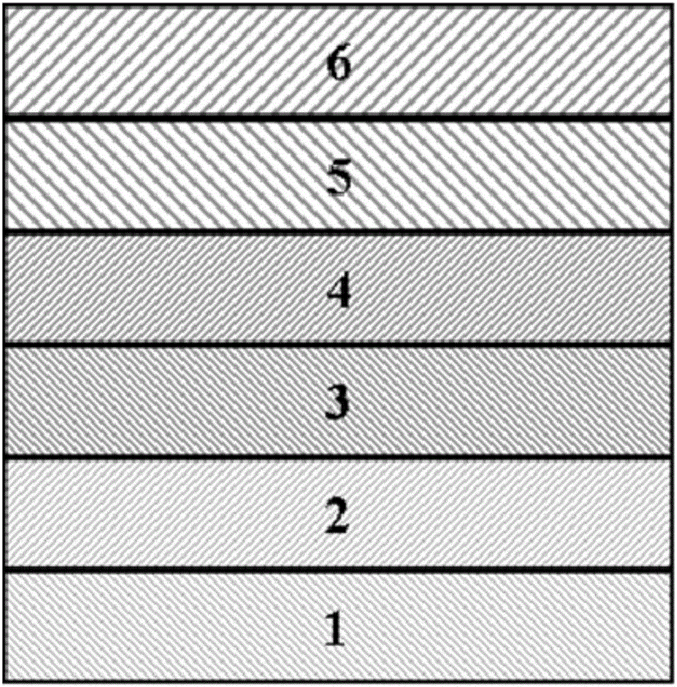
[0036] A perovskite photodetector for accelerated electron filtering (structure shown in figure 1As shown), it sets substrate 1 (glass substrate coated with indium tin oxide), anode 2, hole transport layer 3, active layer 4, electron filter layer 5 and composite cathode 6 layer by layer from bottom to top, Its preparation method comprises the following steps:

[0037] 1) Clean the glass substrate (thickness: 90 nanometers) coated with indium tin oxide (ITO) on the surface (15 minutes ultrasonic cleaning with acetone, 15 minutes ultrasonic cleaning with ethanol), and dry the cleaned glass substrate with a nitrogen gun , followed by UV sampling treatment on the ITO surface (processing for 20 minutes);

[0038] 2) Deposition of the hole transport layer on the ITO surface of the glass substrate processed in step 1): the hole transport layer material used is PEDOT:PSS, which is spin-coated on the ITO surface at a rate of 4000 revolutions per second for 30 seconds, and then place ...

Embodiment 2~3

[0046] The structure and preparation method of the perovskite photodetector for accelerated electron filtering described in Examples 2 and 3 are roughly the same as in Example 1, except that the mixing ratios of PC71BM and the exciton blocking material TmPyPB are 40:60 and 60, respectively. : 40, the spectral responsivity of embodiment 1~3 gained perovskite photodetector is with the variation relation of mixing ratio such as Figure 6 shown.

Embodiment 4

[0048] The structure and preparation method of the perovskite photodetector for accelerated electron filtering described in Example 4 are roughly the same as in Example 1, except that the exciton blocking material used is replaced by OXD-7, and the obtained perovskite photodetector The spectral responsivity see Figure 7 , the results show that the use of OXD-7 as an exciton blocking material also exhibits a high spectral responsivity.


PUM

PropertyMeasurementUnit
Thicknessaaaaaaaaaa
Thicknessaaaaaaaaaa

Abstract

The invention discloses a perovskite photoelectric detector for accelerating electron filtering. The perovskite photoelectric detector comprises a substrate, an anode, an active layer and a compound cathode, wherein a hole-transporting layer is arranged between the anode and the active layer and an electron filtering layer is arranged between the active layer and the compound cathode. According to the invention, a perovskite material, which is characterized by high migration rate, low exciton binding energy, longer exciton life and longer exciton diffusion length, is taken as the active layer of the photoelectric detector, so that the loss of heat exciton in the device is greatly reduced. A novel electron filtering layer is creatively provided; the electrons can be effectively transmitted to the cathode and then collected; the recombination probability of exciton and the quenching effect of electrode to exciton can be greatly reduced; the obtained perovskite photoelectric detector has higher external quantum efficiency and spectral responsivity; the performance is obviously promoted.

Description

technical field [0001] The invention belongs to the field of organic optoelectronics, relates to a novel photodetector, in particular to a perovskite photodetector with a high-efficiency filtering electronic structure. Background technique [0002] Organic photodetection devices have attracted extensive research interest due to their advantages such as low fabrication cost, wide range of material sources, light weight, flexibility, and easy integration with other optoelectronic devices. A large number of studies have proved that organic photodetectors have very broad application prospects in industry, agriculture and social life. In recent years, although the relevant scientific research has made great progress, the performance of the device has been greatly improved, but limited by some defects of the organic material itself and some problems in the structure design of the existing device, the performance of the device Ascension progress is slower. Therefore, the developm...

Claims


Application Information

Patent Timeline
IPC IPC(8): H01L51/42
CPCH10K85/215H10K85/30H10K30/451Y02E10/549
Inventor 薛钦易建鹏谢国华
Owner HUAZHONG NORMAL UNIV
Why Eureka
Try Eureka