PCB and differential wiring impedance matching optimization structure thereof

A technology for optimizing structure and line impedance, applied in the direction of electrical connection printed components, printed circuit components, electrical components, etc., can solve problems such as impedance discontinuity

Pending Publication Date: 2020-10-02
INSPUR BUSINESS MACHINE CO LTD
View PDF4 Cites 5 Cited by
  • Summary
  • Abstract
  • Description
  • Claims
  • Application Information

AI Technical Summary

Problems solved by technology

[0007] The purpose of the present invention is to provide a differential wiring impedance matching optimization structure, which can avoid the problem of impedance discontinuity caused by the differential transmission

Method used


Image

  • PCB and differential wiring impedance matching optimization structure thereof
  • PCB and differential wiring impedance matching optimization structure thereof
  • PCB and differential wiring impedance matching optimization structure thereof

Examples


Embodiment Construction

[0022] The following will clearly and completely describe the technical solutions in the embodiments of the present invention with reference to the accompanying drawings in the embodiments of the present invention. Obviously, the described embodiments are only some, not all, embodiments of the present invention. Based on the embodiments of the present invention, all other embodiments obtained by persons of ordinary skill in the art without making creative efforts belong to the protection scope of the present invention.

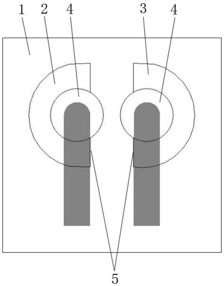
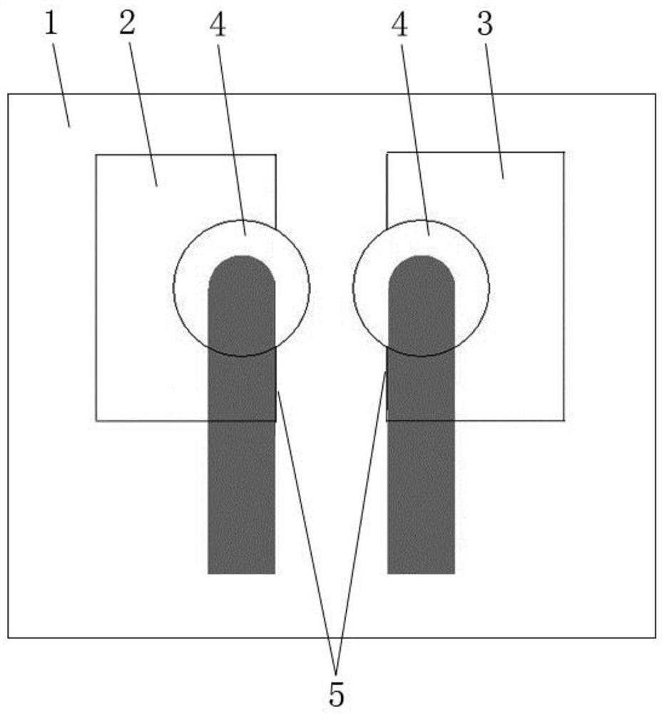
[0023] Please refer to figure 1 , figure 1 It is a schematic diagram of the overall structure of the first specific embodiment provided by the present invention.

[0024] In the first specific implementation manner provided by the present invention, the optimized differential wiring impedance matching structure mainly includes a substrate 1 , a first pad 2 , a second pad 3 and a layer change hole 4 .

[0025] Among them, the substrate 1 is the main structure...


PUM


Abstract

The invention discloses a differential wiring impedance matching optimization structure, which comprises a substrate; a first bonding pad and a second bonding pad which are arranged on the surface ofthe substrate; and layer changing holes which are formed in the first bonding pad and the second bonding pad and used for differential wiring, wherein the opposite sides of the first bonding pad and the second bonding pad are each provided with a notch used for reducing the hole distance between every two adjacent layer changing holes. Thus, the areas of the opposite sides of the first bonding padand the second bonding pad are cut off at the same time through the notch design, so that the distance between the layer changing holes can be shortened; and the differential cables can be close to each other when outgoing, and the differential wiring mode approaches to a long straight parallel line, so that the problem of impedance discontinuity caused by layer-changing wiring of the differential transmission cable can be avoided, the impedance matching rate of the whole differential wiring is improved, the differential signal loss is reduced, and meanwhile, the occupation of the differential wiring on the PCB wiring space can be reduced. The invention further discloses a PCB, and the beneficial effects of the PCB are as described above.

Description

technical field [0001] The invention relates to the technical field of PCB, in particular to an optimized structure for differential trace impedance matching. The invention also relates to a PCB board. Background technique [0002] With the development of the electronics industry, more and more electronic devices have been widely used. [0003] In the field of PCB technology, the development of PCB has become increasingly mature. As the signal transmission rate continues to increase, the wiring density of the server PCB board is also getting higher and higher, and the requirements for signal loss are also getting higher and higher. How to reduce signal loss has become a very critical issue in current design, among which, punching holes in the routing of high-speed signals is a very important influencing factor. [0004] At present, the high-speed signal lines on the server PCB board are generally routed in a differential routing manner. Differential transmission is a sig...

Claims


Application Information

Patent Timeline
IPC IPC(8): H05K1/02H05K1/11
CPCH05K1/0245H05K1/025H05K1/111H05K2201/0776
Inventor 曹颖男
Owner INSPUR BUSINESS MACHINE CO LTD
Why Eureka
Try Eureka